Wafer silicon
Wafer silicon :There are primarily two types of silicon wafers in use today. There are two types of silicon wafers: undoped silicon
Wafer silicon
Free Standing gan Wafer | Single Crystal Substrates
Si Doped Undoped Laser Device Gallium Nitride Wafer
300mm Gan Wafer | Gallium Nitride Wafer For Power Micro LED
8 Inch 12 Inch 6Inch gan Wafer
2 Inch 4 Inch GaN Wafer | Gallium Nitride Wafer
4inch 6inch GaN-ON-SiC EPI layer
Wafer silicon
The Benefits of Wafer Silicon for Integrated Circuits
Your integrated circuits’ performance can be enhanced by using wafer silicon. This is as a result of the characteristics present in this substance. These include reflective optics and infrared (IR).
built-in circuits : Wafer silicon
Electronic devices in small are known as integrated circuits (ICs). In essence, they are a collection of semiconductors that have been wired together and stacked in layers. They might be as complicated as full microcomputers or as simple as logic modules. ICs are found in a wide variety of microelectronic devices, including digital watches, moon-landing rockets, and pocket calculators.
The creation of a single silicon crystal is the first stage in the creation of an integrated circuit. Following that, thin wafers of this crystal are cut. A wafer typically has a diameter of 300mm. These wafers are employed in tire pressure sensor systems, mobile devices, and even computer circuits.
The silicon is then exposed to chemicals. The so-called “doping elements” are subsequently blasted into the wafer. Arsenic, phosphorus, and gallium are the doping substances. These doping substances aid in regulating the silicon wafer’s physical characteristics.
The wafer is polished to smooth out any rough edges after doping. The wafer’s surface is then exposed to light. The wafer’s surface is then covered with a thin coating. The term “resist film” refers to this thin film. The thin film is then exposed to a pattern.
The wafer is then etched. Part of the thin film layer that is not covered by the resist film is removed during this etching process. Each next layer goes through the same procedure. A final passivation layer is subsequently applied to the layer. The final passivation layer seals the surface and stops water from penetrating the wafer. The wafer is then placed inside a plastic bag that is anti-static.
The wafer is then positioned beneath the first layer mask. This mask is clear in certain places and opaque in others. Images of many hundred ICs are included. Additionally, the circuits are tested using this mask.
The wafer is then split into thousands of separate IC pieces. Die sizes are too small for soldering. A sturdy plastic container holds the dies. Connection pins in the packaging could be made of metal or ceramic.
Then, these parts are examined to make sure they work properly. After that, a dual-inline packaging in black is used to house the chips. Thin wires, which may be made of gold or aluminum, are used to connect them to the package’s outside pins.
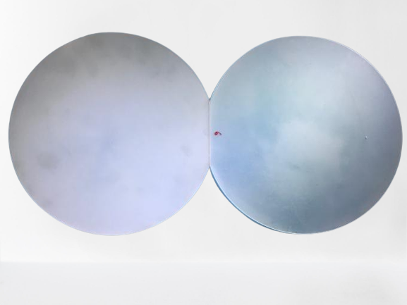
Mirror optics : Wafer silicon
High spectral translucency optical grade silicon wafers are a potential material for semiconductor applications. In the ultraviolet, visible, and near infrared spectral bands, they display exceptional transparency. They come in both monocrystalline and polycrystalline varieties. They are created via a chemical process.
There are many different applications for optical grade silicon wafers, including photonic devices. They can be found in locations with flat, continuous taper, and arcuate taper. Additionally, they have powerful angular functions.
Solar cells can use optical grade silicon wafers with a very high spectral translucency. They are also perfect for laser aiming applications and photonic devices. They require transmission above 50% in the 1.5 to 6 micron wavelength region, as well as a relatively high resistance of at least 20 ohm-cm.
On porous silicon, precise control of the refractive index and thickness is necessary for high-quality optical devices. Single- and double-layer AR coatings have been shown to be most efficient for these applications when used at frequencies around 250 GHz. Deep Reaction Ion Etching has been used to create this covering. On silicon wafers with high resistivity, it was tested.
Near infrared wavelengths are less likely to be reflected thanks to a new coating that is 700 nm thick. The updated coating also reduces sunlight reflection. This coating can be customized in size.
The new coating may also be placed over a vast area and is extremely thin. It can also reach new transmittance heights. Additionally, it is quite useful for reducing Fresnel reflection on the silicon sheet.
Infrared optical devices can be made out of silicon for incredibly little money. However, its infrared transmission is constrained by high water absorptions. Additionally, because its absorption is not constant across the spectrum, it exhibits a lengthy tail at very long wavelengths. It is therefore inappropriate for the collecting of pyrometer readings.
The material needs to be thin and have outstanding transmission properties in order to produce high-quality reflected optics on silicon wafers. The substance should also have low resistance and good thermal characteristics. Silicon wafers are produced in vast quantities and as cylindrical elements to meet these specifications. They are easily accessible with IR spectroscopy modifications.