sic wafer
sic wafer : If you’re interested in finding out more about sic wafer, you’ve come to the right place. We are a professional supplier of sic substrate products in China. You’ll learn about its process and cost here. After reading this article, you’ll be well-equipped to choose a silicon carbide wafer for your next project. Please contact us now, and we will shorten your purchase and understand the progress of this product. Our products include 6 inch sic wafer , 4h sic wafer
Free Standing gan Wafer | Single Crystal Substrates
Si Doped Undoped Laser Device Gallium Nitride Wafer
300mm Gan Wafer | Gallium Nitride Wafer For Power Micro LED
8 Inch 12 Inch 6Inch gan Wafer
2 Inch 4 Inch GaN Wafer | Gallium Nitride Wafer
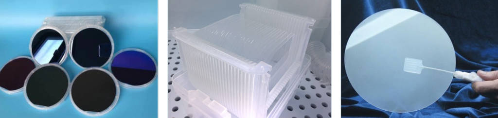
4inch 6inch GaN-ON-SiC EPI layer
sic wafer
Silicon carbide has been used in various applications due to its excellent properties, such as its hardness, high temperature resistance, chemical resistance, and high thermal conductivity.
It is utilized in the production of polished wafers. These wafers are thin, disc-shaped single crystal silicon carbide products that are created through a process known as physical vapor transport, using high-purity SiC crystals.
The grinding of SiC wafer processing is utilized by a diamond slurry. This step plays a crucial role in preparing the wafers for subsequent stages.
Once the desired flatness is attained, the wafers undergo mechanical and chemical polisher to obtain mirror-surface finishes. This meticulous polishing sic wafer processing ensures that the SiC wafers exhibit optimal smoothness and surface quality.
With its exceptional thermal conductivity and ability to withstand high operating temperatures, SiC wafers are capable of efficiently dissipating heat and maintaining stable performance under demanding conditions.
These properties, combined with its superior hardness and chemical resistance, make SiC wafers highly sought-after for cutting-edge technologies that require robust and reliable semiconductor components.
What are Silicon Carbide (SiC) Wafers & Substrates?
Wafers and substrates derived from silicon carbide are specialized materials that play a pivotal role in semiconductor technology. SiC wafers is their high thermal conductivity. This enables efficient heat dissipation. It is well-suited for high-power electronic devices that generate significant heat during operation like LED lights.
SiC wafers possess excellent mechanical strength and has a wide bandgap. SiC’s wide bandgap allows for higher voltage operation. Devices based on SiC wafers to operate beyond the capabilities of traditional materials such as silicon or gallium arsenide.
The unique combination of high thermal conductivity, excellent mechanical strength, and wide bandgap sets SiC wafers apart as a compelling choice for semiconductor technology.
Silicon Carbide as a Semiconductor
Silicon carbide has emerged as a remarkable semiconductor material, offering distinct advantages over traditional semiconductors like silicon. Sic wafer has higher breakdown electric field strength compared to silicon.
It can withstand electric fields that are ten times stronger. Enhanced breakdown electric field strength allows for the design and development of compact devices that can handle higher power levels without compromising performance or reliability.
The wider band gap contributes to SiC’s superior performance in terms of thermal conductivity, efficiency, and overall power handling capabilities. SiC wafers offer greater flexibility in terms of p- and n-type control, which is crucial for device construction. SiC allows for precise control over both types of carriers.
Advantages of Silicon Carbide
SiC wafers offer a host of advantages that make them highly desirable for a wide range of applications. The unique properties of SiC wafers contribute to improved performance, enhanced reliability, and reduced cooling requirements.
Hardness
SiC wafers exhibit exceptional hardness, which enables the fabrication of smaller die sizes while maintaining the same breakdown voltage. This characteristic is particularly advantageous in applications where space is limited, or miniaturization is a priority.
Additionally, the hardness of SiC wafers contributes to their excellent thermal management properties. The efficient dissipation of heat helps reduce cooling requirements and enhances the overall performance and reliability of electronic devices.
Thermal Capabilities
SiC wafers possess impressive thermal capabilities due to their high dielectric breakdown intensity. Compared to silicon, SiC wafers can withstand electric fields that are approximately ten times higher. This feature is crucial in high-voltage applications where the ability to handle elevated electric field strengths is paramount.
The higher breakdown voltage of SiC wafers reduces the turn-on resistance that occurs at high breakdown voltages, enabling improved performance and efficiency in power electronic devices.
Insulation
SiC wafers behave like electrical insulators at high breakdown voltages, minimizing undesirable leakage currents and improving the overall performance of the devices.
The enhanced thermal capabilities of SiC wafers also allow them to operate at higher frequencies and temperatures without compromising reliability.
Silicon Carbide (SiC) Wafers & Substrates Applications
SiC wafers and substrates have extensive applications in various electronic devices. The unique properties of SiC wafers make it particularly suitable for various applications that require high-power capabilities, high-frequency operation, and efficient energy conversion.
Applications of SiC wafers is in the fabrication of electronic devices such as power diodes. SiC-based power diodes offer significant advantages over traditional silicon diodes, including lower switching losses, higher breakdown voltage, and enhanced thermal management.
SiC wafers are used in the production of MOSFETs and FET devices. SiC-based MOSFETs and FETs exhibit exceptional performance, including high breakdown voltage, low on-resistance, and fast switching speed. These attributes make them well-suited for power electronics applications that demand high efficiency, reduced losses, and compact designs.
SiC wafers are employed in the development of high-power microwave devices and RF (Radio Frequency) transistors.
The superior thermal conductivity and high-frequency capabilities of SiC enable the fabrication of high-performance microwave and RF devices. These devices find application in wireless communication systems, radar systems, satellite communications, and high-frequency amplifiers, among others.
Silicon Carbide (SiC) Substrate and Epitaxy
SiC epi wafer manufacturing process is depositing SiC materials onto either bare wafers or as part of the transistor device fabrication. This process allows for the precise control of layer thickness, ranging from sub-micron levels to over 200μm.
Such versatility in layer thickness enables the SiC substrate manufacturers of customization of SiC-based devices to meet specific requirements in terms of performance, power handling capabilities, and integration into complex circuits.
The epitaxial growth of SiC layers on SiC substrates offers several advantages. It ensures a high-quality interface between the epitaxial layer and the substrate.
This can result in improved crystal structure and material purity. This enhances device performance, reduced defect density, and increased reliability.
SiC epitaxial wafer enables the fabrication of complex transistor structures. By selectively depositing different materials with specific doping profiles. It becomes possible to create both n-type and p-type regions within the epitaxial layers.
This flexibility is crucial for constructing various semiconductor devices, including diodes, MOSFETs, and transistors.
The use of SiC substrates in epitaxy also eliminates the need for transferring the sic epitaxial wafer layers from one substrate to another. SiC substrates provide a stable and compatible foundation for epitaxial growth. This affects the integrity, quality of the deposited layers and SiC substrate price.
How Do You Choose Silicon Carbide Wafers & SiC Substrates?
When choosing silicon carbide wafers and SiC substrate supplier for your specific application, several key factors should be taken into consideration. Determine the desired electrical properties of the SiC material and select appropriate dopants accordingly.
Common dopants used in SiC include nitrogen and aluminum. The choice of dopants influences the conductivity type (n-type or p-type) and the level of carrier concentration in the material.
Evaluate the available wafer SiC, wafer size to ensure compatibility with your fabrication process. There are 2 inch, 4 inch, 6 inch and 8 inch sic wafer. Assess the surface roughness of the SiC wafers, typically measured in root mean square (RMS) values.
Low roughness values, such as RMS <1 nm, are desirable to prevent issues during deposition or device fabrication processes.
Determine the desired crystal orientation of the SiC wafers. Common orientations include 4H-SiC wafer and 6H-SiC wafer. The crystal orientation affects the physical and electrical properties of the material, including its bandgap, mobility, and breakdown voltage.
Determine the required thickness of the SiC wafers based on both mechanical and electrical considerations. Consider the resistivity range of the SiC material to ensure it matches the intended electrical behavior for your application. Also consider the SiC wafer cost as well. These properties and characteristics all affects the SiC wafer price.
Difference Between Prime and Research Grade Silicon Carbide Wafers
Prime grade silicon carbide wafers are manufactured with stricter specifications and tighter tolerances. These sic wafer fabrication is especially manufactured for electronic devices.
Prime grade wafers exhibit superior material properties, such as uniform crystal structure, low defect density, and high purity.
Research grade silicon carbide wafers are primarily used for research and development purposes. They have more relaxed tolerances and specifications compared to prime grade wafers.
Research grade wafers are often employed in feasibility studies, process development, and initial testing phases where the exacting requirements of device fabrication are not the primary concern. These wafers may have slightly higher defect densities or variations in material properties compared to prime grade wafers, but they still provide valuable insights and data for research purposes.
High Crystal Quality for Demanding Power Electronics
SiC wafers offer exceptional crystal quality. This makes them well-suited for demanding power electronics applications. While silicon wafers possess near-perfect crystallinity, they face limitations when it comes to certain power electronic devices. This due to the lattice mismatch between gallium nitride and silicon.
GaN is a wide-bandgap semiconductor material known for its high electron mobility and power efficiency. The lattice mismatch between GaN on sic substrate poses challenges when integrating these materials directly on silicon wafers. The significant 17% lattice mismatch can result in defects, strain, and dislocations. This can degrade the performance of power electronic devices.
SiC wafers offer a solution to overcome the lattice mismatch issue between GaN on SiC substrate. SiC has a closer lattice match with GaN compared to silicon. This reduces the strain and enabling higher crystal quality in GaN-based power electronic devices. The high crystal quality of SiC wafers translates into improved material integrity.
Process
Several steps are involved in the fabrication of SiC wafers, including dicing and polishing. The various dicing steps require varying feed rates and spindle speeds. This process yields a wafer with a relatively smooth surface and low roughness. The process also increases yield.
The final major step in the SiC wafer production process is chemical mechanical polishing, which aims to prepare the sic substrate surface for epitaxial growth while causing minimal shape change. To remove only a few microns from the surface of the wafer, this process typically employs a chemically reactive slurry and a polyurethane-based polishing pad. A template or vacuum chuck with a backing film holds the SiC wafer in place.
This process, in addition to annealing, checks for crystal defects. These flaws can have a negative impact on the semiconductor’s performance. The silicon carbide wafers that result are then sliced into individual chips. This manufacturing process ensures higher quality and efficiency, as well as the ability to meet specific customer requirements.
An important parameter for SiC dicing is the dicing blade. It is critical to select one with a resin-bonding blade. This blade is designed specifically for SiC dicing. Furthermore, it is critical to select a spindle speed that reduces blade vibration.
Properties
A photomicrograph of the properties of an EDM-treated gan wafer . This material is highly conductive and has a high thermal conductivity. This material has a smooth surface microstructure as well.
SiC wafers are among the best semiconductor materials on the market today. Its superior electrical and thermal properties make it ideal for a wide range of electronic devices. It has a high resistance to thermal and electrical radiation and can be used in a variety of power and voltage applications. Silicon carbide wafers are widely used in power conversion and have many other applications.
To make high-quality gan wafer , the silicon substrate must first be prepared. The silicon wafer is oxidized during this process, and the number of dislocations and scratches on the surface is reduced. This process will make your SiC wafer thinner than standard semiconductors. However, specialized tools will be required for the job.
Another distinguishing feature of SiC is its low field mobility. It has superior electrical properties to SiO2 and is frequently used in power devices. Device simulation technologies are required for the design and manufacture of SiC power devices.
Applications
SiC is a common material used in high-temperature applications. It can withstand temperatures as high as 2700 degrees Celsius. It is used in bulletproof vests, light-emitting diodes, and extruders. It is also known as carborundum. It is also used in electronic devices that require high voltages.
SiC wafers are widely used in power semiconductor applications. Because of their high thermal and electrical conductivity, they are an excellent choice for these applications. They can also withstand high temperatures without overheating. Because of these characteristics, SiC wafer microfabrication is a viable platform for manufacturing products in harsh environments.
The automotive industry is another application for SiC wafers. Gan wafer are used in automotive technology as a silicon substitute for a variety of purposes, including lowering the cost of driving range per charge, speeding up charging, and increasing fuel efficiency. This material is also used in battery technology in the automotive industry.
Silicon carbide is a chemical compound that is made up of silicon and carbon. It occurs naturally in the form of and possesses a number of properties that make it a valuable semiconductor material. Silicon carbide has excellent thermal conductivity, oxidation resistance, and mechanical strength. SiC wafers are the ultimate solution for power electronics due to their excellent optical properties.