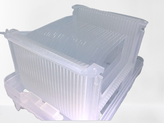
4 Inch 6 Inch Gan Wafer | Gallium Nitride Wafer
4 Inch 6 Inch Gan Wafer | Gallium Nitride Wafer . At present, GaN wafers are mainly grown from real bulk materials through ATAL Commonweal, and are usually used in LED and transistor products and laser products.

4 Inch 6 Inch Gan Wafer
Wafers with 4inch and 6inch GaN-ON-SiC EPI layers Wafers with GaN-ON-Si EPI layers
Introduced GaN-on-GaN GaN-on-SIC Feature :
4 Inch 6 Inch Gan Wafer | Gallium Nitride Wafer . At present, GaN wafers are mainly grown from real bulk materials through ATAL Commonweal, and are usually used in LED and transistor products and laser products.
GaN epitaxial wafers are classified into four varieties based on their substrates: GaN-on-Si, GaN-on-SiC, GaN-on-Sapphire, and GaN-on-GaN.
GaN-on-Si: The current industry production yield is low, but there is a huge potential for cost reduction: because Si is the most mature, defect-free, and lowest-cost substrate material; at the same time, Si can be expanded to 8-inch wafer fabs, reducing the unit production cost, so that the wafer cost is only one percent of that of the SiC base; the Si growth rate is 200 to 300 times that of the SiC crystal material, and the corresponding GaN-on-Si epitaxial wafers are primarily employed in the fabrication of power electronic devices, with the technical trend toward optimizing large-scale epitaxy technology.
GaN-on-SiC: This material is appropriate for RF because it combines the good thermal conductivity of SiC with the high power density and low loss characteristics of GaN. The current size is still limited to 4 inches and 6 inches due to the SiC substrate, and 8 inches has not been advocated. GaN-on-SiC epitaxial wafers are primarily employed in the fabrication of microwave radio frequency devices.
4 Inch 6 Inch Gan Wafer | GaN-on-sapphire: Mainly utilized in the LED market, the standard size is 4 inches, and GaN LED chips on sapphire substrates have a market share of more than 90%.
Blue/green lasers, which are utilized in laser display, laser storage, laser illumination, and other sectors, are the principal application market for GaN employing homogeneous substrates.
GaN device design and fabrication: GaN devices are classified as radio frequency devices or power electronic devices. Power electronic device products include SBD, normally-off FET, Cascode FET, and other products for wireless charging, power switch, envelope tracking, inverter, converter, and other markets. Radio frequency device products include PA, LNA, switches, MMICs, and other products oriented to base station satellite, radar, and other markets.
It is classified into two types based on the method: HEMT, HBT radio frequency process, and SBD, PowerFET power electronic device process.
Applications
– LEDs of several colors: white, violet, ultraviolet, and blue.
– Environmental monitoring
MOCVD epitaxial growth substrates, for example
– Laser diodes in violet and green for ultra-small projectors.
– Charge electronic gadgets
– Electronic equipment with a high frequency of operation
Power Device, Laser Projection Display, and so on.
Storage of dates
Lighting that saves energy
Electronic gadgets with high efficiency
New hydrogen energy storage technology
Terahertz light source
Specifications for GaN-on-4 Inch 6 Inch Gan Wafer | GaN Substrates for Each Grade
| 4-6”GaN ON-SIC | |
| Item | Type: N-type SIC |
| Dimensions size | Ф 100.0mm ± 0.5mm |
| Thickness of Substrate | 350 ± 30 µm |
| Orientation of Substrate | 4°off C-axis(0001) |
| Polish | DSP |
| Ra | <0.2nm |
| Epilyaer structure | 0.5um pGaN/20um iGaN/2um nGaN/FS-GaN |
| Epi thickness/STD | 1~25um/<3% |
| Roughness | <0.5nm |
| Discolation density | <1X107cm-2 |
| pGaN Carrier concentration | >1E17CM-3; |
| iGaN Carrier concentration | > 1E17CM-3; |
| nGaN Carrier concentration | >1E17CM-3; |
| Useable area | P level>90%; R level>80%: Dlevel>70%(edge and macro defects exclusion) |
4 Inch 6 Inch Gan Wafer | Gallium Nitride Wafer
When you want to look for 2 double side polished sapphire wafer, if you will search those keywords to found us ? Such as 2 inch sapphire wafer,2 inch sapphire wafer price,2 inch sapphire wafer thickness,2 sapphire wafer, double-side polish 2 sapphire wafer etc ?