Magnesium Oxide Wafer Supplier & Manufacturer in China
Magnesium Oxide Wafer : A basic material used as a thin film and single crystal, it is a highly transparent raw material, and its cost is very cost-effective. In many application fields, magnesium oxide is widely used, mainly for some high-temperature superconducting thin film coatings and as a sturdy and lightweight material, which is relatively low-cost in production. Therefore, it is the first choice for the material when selecting raw materials for thin film substrates.
2 Inch A - Axis Sapphire Wafer For EPI
5 Inch Sapphire Wafer R Plane Dia 125mm
8 Inch Sapphire Wafer Dia 200 mm
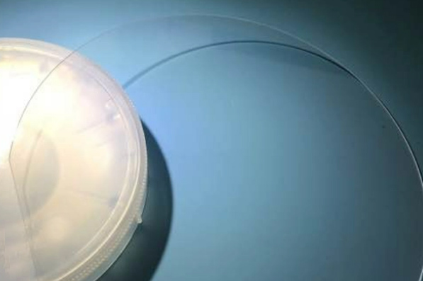
Magnesium Oxide Single Crystal Wafer
12 Inch Sapphire Wafers Dia 300mm
4 inch Sapphire Wafer C-Plane Single or Double Side Polish Al2O3 Single Crystal
6 inch Sapphire Wafer C-Plane Single or Double Side Polish Al2O3 Single Crystal
MgO, Magnesium Oxide Single Crystal Substrates
Magnesium Oxide Wafer
There is no special phenomenon in speech, which is that it is not easy to react with other elements in nature, which makes it have a good characteristic of corrosion resistance. At the same time, its thermal conductivity is also a major advantage.
It is a semiconductor raw material, and it also has a low melting point, very heat and corrosion resistance. Magnesium oxide is transparent to all kinds of light, which is only a small part of the advantages of magnesium oxide chips.
Circular and square are two shapes of magnesium oxide wafers, which can also be divided into flat and non flat single-sided polishing or double-sided polishing. The size range is also relatively wide, usually between two inches and 12 inches.
We can also provide thickness according to customer requirements, usually between one millimeter and two millimeters, 0.4 millimeters and 0.5 millimeters, and the surface roughness is very low. Our magnesium oxide chip has an extremely high surface finish, transparency, and thermal conductivity, making it a very popular semiconductor raw material.
Main advantages and characteristics.
- The density is indeed depressed.
- High quality crystal.
- It can be used to improve the scale of semiconductor manufacturing.
- The tolerance range applicable to some specific equipment manufacturing requirements.
- It can optimize the performance and cost control of power electronic equipment.
Magnesia wafer is also a ceramic material, which has a relatively good mechanical performance, and can be evenly heated or cooled to avoid thermal shock. Its operation is good. It provides the performance for aluminum oxide, and can maintain the stability of performance at 2200 degrees.
This is a major advantage of magnesium oxide gold source. It is also widely used in some LED laser diodes and some UV photodetectors, It is very compatible with potassium nitride, and in terms of performance, it can perfectly achieve high-quality defect epitaxial thin films. So we strongly recommend that you use our amazing magnesium oxide.
At present, magnesium oxide has been widely used in the production of high-temperature superconducting films, optical films, magnetic films, and ferroelectric films this year. It can be used to produce high-temperature superconducting Weibo, filters, and other devices required for mobile communication devices. If you also have production needs in this regard, please contact our technical department or sales department, and we will provide you with complete product information.
If you just need Magnesium Oxide Wafer , please contact us immediately.
Magnesium Oxide Wafer