8 wafer
8 wafer :
The KY process used for sapphire crystal growth is currently used by many companies in China to produce sapphire in the electronic and optical industries.
Its high-purity oxidation rate is melted in a boiler with a temperature of more than 2140 degrees. A precisely oriented seed crystal is dipped into the molten alumina. The seed crystal is slowly pulled upwards and may be rotated simultaneously. By precisely controlling the temperature range, pulling speed and temperature decreasing speed,
it is possible to produce a large single crystal pig block similar to a cylinder from the melt.After the single crystal sapphire balls grow out,
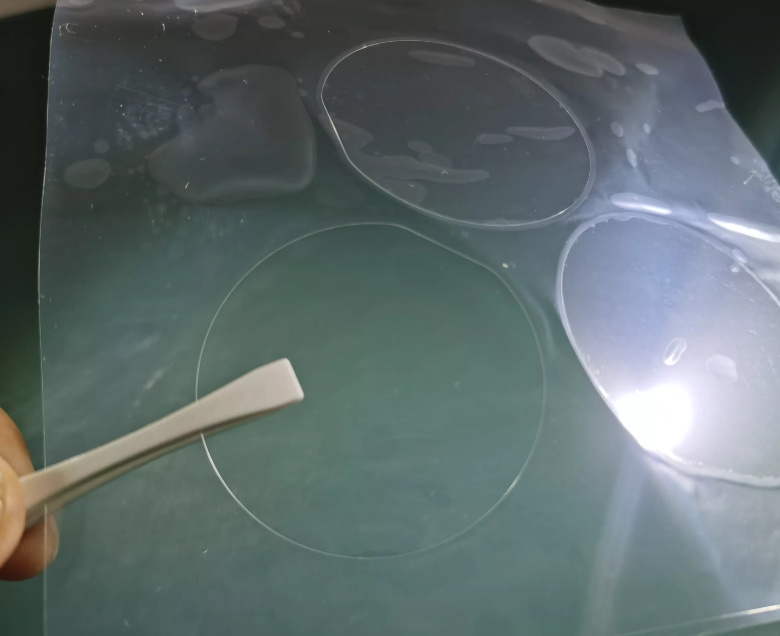
they are cut into the required window thickness by the rods and rods which are made into cylindrical shape by aliens. These rods are cut into the required window thickness and finally polished to the required surface smoothness.
8 wafer
Free Standing gan Wafer | Single Crystal Substrates
Si Doped Undoped Laser Device Gallium Nitride Wafer
300mm Gan Wafer | Gallium Nitride Wafer For Power Micro LED
8 Inch 12 Inch 6Inch gan Wafer
2 Inch 4 Inch GaN Wafer | Gallium Nitride Wafer
4inch 6inch GaN-ON-SiC EPI layer
8 wafer
8 wafer:
Getting the right amount of experience is very important to ensure your project. Whether it is large-scale testing or specific, there are many options for applying it to chips. Before Gome enters the park, well, we have some suggestions for you to save time and money.
Silicon wafers.
Silicon wafers are used as semiconductor materials, microelectronic devices and optoelectronic components. They are used in smart appliances and solar electronics. The smallest silicon chip diameter is usually less than 150 mm. Most silicon chips are used for diodes.
Monocrystalline silicon chips are used for solar electronics with high conversion efficiency. For this purpose, some of our silicon chips are manufactured along the shortcut plane.
If microcracks appear on the wafer, it may lead to wafer training, so it is important to choose the correct wafer growth method.
Mechanical specification Wafer.
There are several types of mechanical elements, and these experiences can be used in various equipment. The most common is 300 mm Wafer. However, this resource has been produced into various shapes and sizes.
One of the most common uses of these silicon chips is as a shielding material for precision tools and instruments. Silicon is an extremely reliable material that can be used for this purpose. Its high heat resistance makes it useful in the aviation industry. Silicon is a good substrate for semiconductor materials.
Silicon wafers have a variety of diameter products, which can be as small as 25mm to 450mm, but it takes a lot of time and engineering to develop silicon wafers with a diameter of 450mm.