200mm sic wafers Supplier & Manufacturer in China
200mm sic wafers : We are a professional manufacturer of 200mm sic wafers in China.
Our silicon carbide wafer is an advanced semiconductor material, which can be applied to some environments with strict requirements for high crystal quality of power electronic products.
At present, with the continuous development of transportation energy and industrial market, people’s demand for power electronic products with high reliability and high performance ratio is increasing. In order to meet this demand, we continue to develop new ones. Broadband gap semiconductor materials.
2 Inch A - Axis Sapphire Wafer For EPI
5 Inch Sapphire Wafer R Plane Dia 125mm
8 Inch Sapphire Wafer Dia 200 mm
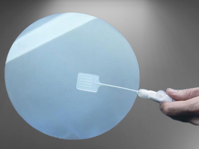
200mm sic wafers | SiC Substrate (150mm, 200mm)
12 Inch Sapphire Wafers Dia 300mm
4 inch Sapphire Wafer C-Plane Single or Double Side Polish Al2O3 Single Crystal
6 inch Sapphire Wafer C-Plane Single or Double Side Polish Al2O3 Single Crystal
200mm sic wafers | 200mm Diameter SiC Wafers
Our silicon carbide wafer provides equipment manufacturers with a relatively high quality substrate. Its advantage is that it can be used to develop high performance power equipment.
The silicon carbide substrate is produced by using relatively advanced physical vapor transmission production technology and some auxiliary means, with high quality convert ingots into wafers.
Main advantages and characteristics.
- The density is indeed depressed.
- High quality crystal.
- It can be used to improve the scale of semiconductor manufacturing.
- The tolerance range applicable to some specific equipment manufacturing requirements.
- It can optimize the performance and cost control of power electronic equipment.
Compared with the size of 150 mm wafer, the size of our 200 mm wafer enables manufacturers to take advantage of higher economies of scale.
Our 200 mm silicon carbide wafer provides consistent mechanical and chemical properties to ensure compatibility and matching with existing and developing equipment manufacturing processes.
To produce high quality 200 mm silicon carbide wafers is a way for us to provide quality assurance for many users. Whether it is 150 mm to 200 mm, we can provide stable quality and high performance quality.
What is the size of silicon carbide wafer? Generally speaking, the standard diameter range of silicon carbide wafers is 25.4 mm, that is, one inch, to 300 mm, that is, 11.8 inches.
We can produce wafers of various thicknesses and directions, and can perform single sided polishing and double sided polishing, even non–olishing services, and can contain dopants.
How many chips can a 200 mm wafer have?In fact, each police officer can basically process more than 150 chips on a 200 mm wafer, and each chip can contain many user designs.
These chips can be better copied, and can also be copied in different sizes on the wafer. When processing in a single batch, the cost of 25 wafers can be reached, which is almost the same as processing a single gold source.
So in order to reduce the cost, we recommend you increase your number.
The use of silicon carbide wafers is actually very extensive. It is mainly used to manufacture high voltage and high power atomic devices, such as diodes, power transistors and high power microwave devices, and so on.
We can list them in detail in the next article.
If you just need 200mm sic wafers , please contact us immediately.