Glass Carrier Wafer |Supplier & Manufacturer in China
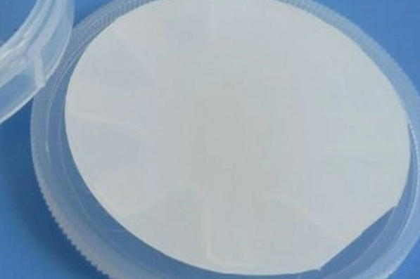
Glass Carrier Wafer : When selecting high-quality glass materials, we carefully cut and shape them, and complete this production. It is a precise and thin glass disc that undergoes many processes to improve the flatness of the carrier wafer. At the same time, we use advanced measurement equipment to test its quality.
The Glass Carrier Wafer is mainly used in some microelectromechanical systems and electronic devices, and of course, it is also a major application scenario in semiconductors. The wafer used is mainly glass carrier, which is used as a temporary bonding machine plate for processing thin semicondafers withs Glass Carrier Wafer has been proven to be an essential element of IC structure.
2 Inch A - Axis Sapphire Wafer For EPI
5 Inch Sapphire Wafer R Plane Dia 125mm
8 Inch Sapphire Wafer Dia 200 mm
Glass Carrier Wafer | glass slide carrier wafer
12 Inch Sapphire Wafers Dia 300mm
4 inch Sapphire Wafer C-Plane Single or Double Side Polish Al2O3 Single Crystal
6 inch Sapphire Wafer C-Plane Single or Double Side Polish Al2O3 Single Crystal
Glass Carrier Wafer | glass wafer carrier
After precise processing, the glass carrier wafer has become a temporary carrier for a very thin semiconductor wafer, which can provide many advantages.
This is a low-polluting raw material.Because it is a highly pure glass carrier, especially in high-temperature processes, it has very little pollution to semiconductor wafers. Its advantages of chemical inertness and cleanliness are all significant reasons for its application in some scientific and industrial fields.
Glass carrier wafers can effectively protect me from damage, scratches, and damage during the handling, transportation, and processing of semiconductors this year. This is particularly important for some very thin application environments or for some easily broken gold elements.
In some lithography fields. The glass carrier provides a durable and flat surface for lithography and patterning of very thin gold gardens, which allows for further processing of experiences that are too thin to be processed separately.At the same time, the glass carrier can handle both sides of the semiconductor wafer simultaneously, without the need for special process treatment, avoiding potential risks of damage and additional process steps.
Main advantages and characteristics.
- The density is indeed depressed.
- High quality crystal.
- It can be used to improve the scale of semiconductor manufacturing.
- The tolerance range applicable to some specific equipment manufacturing requirements.
- It can optimize the performance and cost control of power electronic equipment.
This type of glass carrier has a lower wafer cost, and compared to other equivalent products, the experience of glass carriers provides a more economical solution, which can achieve thinning and double-sided processing of semiconductor wafers, which are particularly prominent technical advantages.
The glass carrier wafer provides a cost-effective solution for protecting, thinning, and handling fragile gold sources during the manufacturing process. They use more advanced processing methods on wafers that are too full to support independently, but there are limitations on the maximum temperature and heating rate. Additional processes are needed to help them solve these difficulties. For some application areas, temporary kneading options can be replaced, Perhaps more suitable.
If you just need glass carrier wafer , please contact us immediately.Looking forward to your inquiry.