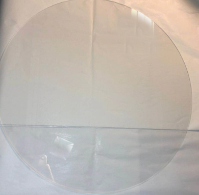
Lithium Niobate Wafer Supplier & Manufacturer in China
lithium niobate wafer : It can be said that lithium sorbate is currently a widely used and relatively complete active optical material in terms of technology. Our production, not counting your experience, can provide more assistance for you when applying it to industrial and laboratory research fields.Lithium niobate is widely used in various fields such as optical light dimming, waveguides and semiconductors, as well as optical fibers. It has a wide transparency range, high electromechanical coupling coefficient for electro-optic and nonlinear optical coefficients, and chemical and mechanical stability.

2 Inch A - Axis Sapphire Wafer For EPI
5 Inch Sapphire Wafer R Plane Dia 125mm
8 Inch Sapphire Wafer Dia 200 mm
Lithium Niobate Wafer | lithium niobate on silicon wafer
12 Inch Sapphire Wafers Dia 300mm
4 inch Sapphire Wafer C-Plane Single or Double Side Polish Al2O3 Single Crystal
6 inch Sapphire Wafer C-Plane Single or Double Side Polish Al2O3 Single Crystal
Lithium Niobate Wafer | Lithium Niobate LiNbO3
lithium niobate wafer
Lithium Niobate Wafer is a widely used rawmaterials used in semiconductor electronics, as well as raw materials commonly used in some optical fields.
There are strong nonlinear optical coefficients in some high optical nonlinearity, which makes the frequency conversion optical parametric oscillation and electro-optical modulation of light possible to be applied LiNbO3.
It also has outstanding performance in the refractive index of light, as it changes with the redistribution of charges caused by light, making it very common and popular in applications such as beam combinations and spatial light modulators.
Main advantages and characteristics.
- The density is indeed depressed.
- High quality crystal.
- It can be used to improve the scale of semiconductor manufacturing.
- The tolerance range applicable to some specific equipment manufacturing requirements.
- It can optimize the performance and cost control of power electronic equipment.
Lithium niobate substrates are increasingly used in some optical devices. By reducing the size of waveguides, several hundred lithium niobates can be used in electro-optical modulators, achieving more widespread applications, such as in driving voltage and expanding high-performance optical devices.
The traditional thickness is generally between 0.5mm and 0.7mm, with an additional 11mm. The standard direction is divided into the x-axis and which direction? There are two types of ingredients: full ingredients and Magnesium doping composition.
In some microwave components, the use of lithium niobate is also very common. Due to its piezoelectric, strong optical, and nonlinear properties, electro-optic effects, and gloss changes, lithium niobate is an important material for various optical and electronic communication and imaging applications. Lithium Niobate Wafer can support light modulators, frequency converters, and some semiconductor fields.
You and the single crystal compound of oxygen form lithium niobate, which is widely used in some mobile phone and other telecom markets. It is a raw material in some surface acoustic wave devices, and is used for selection.
It is also very widely used for other purposes, such as laser frequency doubling, nonlinear optics, Optical parametric oscillator, and many others. Our inventory specifications are very large, It can meet your requirements for delivery time in the shortest possible time.
Our wafer is packaged and tested in crystalline packaging. If you have special requirements, you can inform our technical department about this product.
If you just need lithium niobate wafer, please contact us immediately.