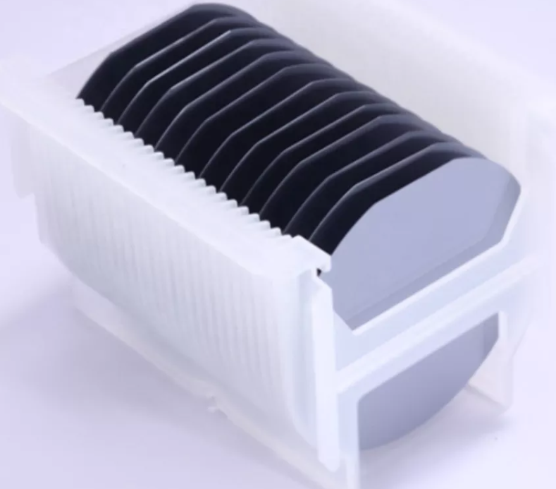
300mm wafer
300 mm wafers are mainly used in the consumer electronics industry, medical vehicles and aerospace. Most chip manufacturers still use 200 mm gold dollars, but some users have started to use 300 mm wafers. Their advantage is lower costs.As a major supplier of silicon wafers in the professional semiconductor industry, our products use high-purity silicon wafers Monocrystalline silicon ingot manufacturing these specified surfaces are very flat and smooth, and they are polished to mirror effect.
300mm wafer
Free Standing gan Wafer | Single Crystal Substrates
Si Doped Undoped Laser Device Gallium Nitride Wafer
300mm Gan Wafer | Gallium Nitride Wafer For Power Micro LED
8 Inch 12 Inch 6Inch gan Wafer
2 Inch 4 Inch GaN Wafer | Gallium Nitride Wafer
4inch 6inch GaN-ON-SiC EPI layer
300mm wafer
300mm wafer:
The characteristic size of a 200 mm wafer is 0.2~0.17 μ m, while that of a 300 mm wafer is 0.14 mm, or even lower.
We can provide you with a wide range of products. Based on 300 mm wafers, we can support the development of today’s semiconductor industry.
Our wafer solutions not only provide 300 mm wafers, but also provide 200 mm wafer.
Now let’s talk about the use of 300 mm wafers? In the semiconductor industry, there are many reasons for the development of a larger 300 mm wafer.
First, the increase in the size of silicon wafers allows each wafer to produce more chips, which is very important because each wafer has more transistors, which means that the cost of each chip will be greatly reduced compared with the products produced in the past.
So the production of integrated circuits is going from 200 mm The number of these fabs is less than 200 mm when transferred to 300 mm, and half of the wafers are produced. This is because 300 mm wafers require fewer work steps, but the cost of processing is relatively low. In spite of this, 300 mm fabs still have a great development direction in the use of memory and image sensors in the next few years.
Compared with the previous large diameter silicon wafers, the single crystal output of 300 mm silicon wafers is higher,
which increases the number of wafers that can be produced on another gold dollar mold.Our 300 mm silicon wafer crystal source attributes include n-type, p-type and non doping.At the same time, we can provide single-sided polishing and double-sided polishing.