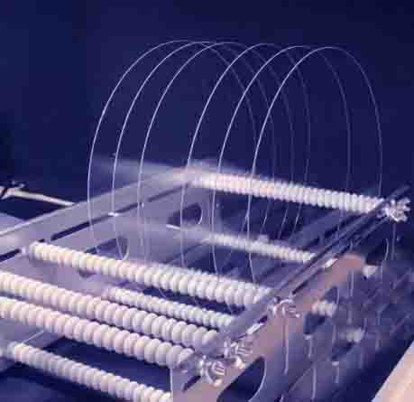
Gan Wafers | High quality Gan Substrates in China
Gan Wafers : XKH is processed using a compound semiconductor method, and the gold element is widely used in many application fields. It can be used in laser diodes and some LED products with special requirements for high brightness, and is widely used in some mobile phone base stations and national defense applications.
Our Gan Wafers include many types: Ntype (undoped), Ntype (Ge doped), and Semi-insulating(Fe doped) substrates are available Non-polar and semi-polar GaN substrates.

Gan Wafers | gan on sapphire wafers
Free Standing gan Wafer | Single Crystal Substrates
Si Doped Undoped Laser Device Gallium Nitride Wafer
300mm Gan Wafer | Gallium Nitride Wafer For Power Micro LED
8 Inch 12 Inch 6Inch gan Wafer
2 Inch 4 Inch GaN Wafer | Gallium Nitride Wafer
4inch 6inch GaN-ON-SiC EPI layer
Gan Wafers | High quality gan epi wafer
Gan Wafers : Gan Substrate comes in many models, including 4 inches, 12 inches, 6 inches, and 8 inches. Of course, we also provide customized sizes for our users.Gan on silicon wafer | with good gan wafer price.
- Material: Single crystal Al2O3 99.999%
- Orientation: C-plane(0001) Off M -axis 0.2°±0.1
- Diameter:76.20±0.2mm or 3inch,2inch,5inch,6inch
- Thickness :500±25um or1000±15um,
- Primary flat 22±1mm
- OF Orientation flat: A axis±0.1°
- Frontside Surface Roughness:Ra<0.3nm
- Backside Surface Roughness: 0.8~1.2um
- ( Or double side polished, both side Ra<0.2nm)
Performance indicators.
Material Sapphire(Al2O3)
Density(20°C) Kg/m3 3.98×10³
Crystal Structure hexagonal
Crystal lattice constant a=4.785Å c=12.991 Å
Mohs hardness 9
Melting Point 2045°C
Coefficient of Thermal Expansion α=5.8×10 -6 /K
Specific heat 0.418W.s/g/k
Thermal conductio 25.12W/m/k(@100°C)
Refractive Index (nd) no=1.768ne=1.76
Tranmission T≈85%(0.3~5um)
At present, Gan Wafers | GaN-ON-silicon is mainly used for LED applications in some power videos. This industrial grade Gan Wafer which the purity reaches 99.9%. It is a type used in low-temperature alloys. Cas No.: 25617-97-4.
In the field of Gan Wafers, we have over 10 years of experience as a Gan Substrate company. In terms of technology, we have involved basic engineering buffer design platforms and crack-free external genitalia structures.
In terms of product level, we are very diverse to meet the needs of different users. The following are some common models we are exporting. If you have any needs in this regard, please contact us promptly.
• GaN-on-Si (up to 300mm)
• GaN-on-SiC (up to 150mm)
• GaN-on-HR_Si (up to 200mm)
• GaN-on-Sapphire (up to 150mm)
• GaN-on-GaN
We mainly produce various sizes of Gan epitaxial wafers on silicon substrates, usually ranging from 100mm to 200mm. The quality meets national standards.
In terms of packaging details, we have chosen cardboard boxes, and the cardboard boxes are 25 pieces, packed in a clean and vacuum box.
The delivery time is 3-20 days, and we will arrange for timely shipment after the deposit for this order.
Please contact our technical or sales department to obtain the price and product information you want.
Whatsapp: 0086-13185071071
A trustworthy wafer supplier.
Gan Wafers | Your Leading Gan Wafer Manufacturer in China
Gan Wafers | High quality Gan Substrates in China
Do you use these keywords to find us? For example gan wafer,gan wafer size,gan epi wafer,gan on silicon wafer,gan wafer market,gan wafer price,gan wafer suppliers,gan on si wafer,gan epi wafer capacity,gan epitaxial wafer,gan hemt wafer,gan on sapphire wafer,gan on si wafer price,gan on sic wafer, and gan wafer,gan wafer cost,gan wafer manufacturer,gan wafer thickness,hemt gan wafer,led gan wafer,typical cost of a 6 gan wafer etc, Anyway, I hope you can finally find us, and we can provide you with professional technical support and price support.