Your Reliable Sapphire Substrate Supplier & Manufacturer
Sapphire substrate:In the whole market, if you want to get a better sapphire substrates price and properties with good composition , and have a better crystal structure, the sapphire of Xinkehui is worth your choice.
Sapphire substrate has a good heat resistance, a wide transmission wavelength range, a unique combination of excellent thermal conductivity and stable electrical performance, and its strength is very high. If you are interested in our sapphire wafer, our large inventory can meet your timely delivery, and if your volume is large, we can have a corresponding discount, We also provide customized sapphire wafer, please go ahead. Love connects with us.
sapphire substrate crystal structure
2 Inch c plane sapphire substrate
Sapphire optical chips, 2inch sapphire wafers for led & Epi
5 Inch Sapphire Wafer R Plane Dia 125mm
5 Inch Sapphire Substrates | Al2O3 Material | 9.0 High Hardness
8 Inch Sapphire Wafer Dia 200 mm
8inch C plane sapphire wafer, Al2O3 crystal optical lens
12 Inch Sapphire Wafers Dia 300mm
1.0mm Double Side Polished Sapphire Crystal Glass Wafers
4 Inch Sapphire Optical Windows A - Axis
85% Vision Light Transmissivity,
Single Crystal for Led
Sapphire Substrate Wafers
China Sapphire Wafer
Over 15 years experience
One-stop Sapphire Wafer supplier & manufacturer
Full Range Varieties of Sapphire Wafer
Good experience cooperating with world-renowned companies
Sapphire Wafer includes 2 inch, 4 inch, 5 inch,6 inch,8 inch, 12 inch etc
Excellent Properties of Sapphire Substrate
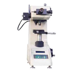
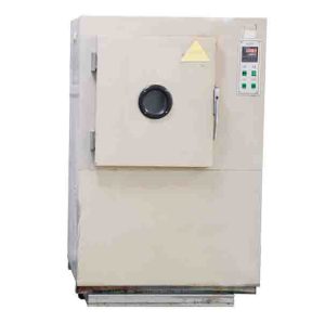
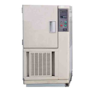
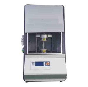
XKH will use specific high-end and advanced testing equipment to test our sapphire related products to ensure that every product you have is efficient and stable.
上一页
下一页
Sapphire Substrate
Do You Experience The Issues When Buying From China
- Hard To Find A Professional aftermarket Sapphire Substrates Supplier & Manufacturer in China,But Foreign Trade Companies Without Guarantee.
- Long Lead Times Of Sapphire Substrate From China,Delivery Time Non – Guaranteed.
- Uneven Quality of Chinese Sapphire Wafer,The Sellers Can not Guarantee The Life Time of Sapphire Wafer.
- Few China Suppliers Can Provide Solutions When You Face Quality Problems
- Rarely Possible To Cooperate with China Factories That Hace Full Service With Strong R & D Team,Manufacturing,Selling, After-Sale Service, And Technical Support.
XKH Will Be Your Trust Sapphire Wafer Supplier
With 15 years of market experience, the Sapphire Wafer of XKH has been recognized by customers in many countries. We are very grateful to users for their support and trust over the years.

Your sapphire wafer products are very good, transparency is very nice , and have a very wide range of applications, especially the price competition. In our market, we have your support, which makes us even more powerful.
John Doe
Vancouver

We have been purchasing sapphire wafers from XKH for 6 years. Their quality has been very stable and delivery has been very timely, especially in terms of technical support. Their engineer team is very strong. We are very grateful for your help.
Jessica Smith
Toronto

In the end, we were lucky to choose Xinkehui as the manufacturer and supplier of our sapphire wafers. Their sapphire wafers are excellent, and our customers are very satisfied with this, especially in terms of price and quality stability. You can purchase from Xinkehui with complete confidence.
Steve Rogers
Montreal
Sapphire Substrates - FAQ
We mainly provide three kinds of sapphire substrates with different surface treatment quality. From the standard sapphire substrate to the polished sapphire substrate with surface quality, the sapphire substrate is basically standard, with a 60~40 appearance and a roughness of about 0.3 nm, which is basically applicable to most spectroscopic and film performance requirements.
When optical transmission is required within the range of ultraviolet or infrared rays, we highly recommend sapphire for your industry. They are ideal substitutes for glass substrates, and have also received very good performance in low temperature optical measurement. Because sapphire substrates have high thermal conductivity, they are also very suitable for use in 2300k high temperature environments.
As a professional sapphire (Al2O3) wafers supplier and provider, we are trusted by most customers all over the world because of our stable quality. Our Sapphire Wafer is also called Al2O3. Its product range includes 1 inch,2inch,3inch,4 inch,5inch,6 inches, which have a large amount of inventory to ensure your timely product needs. We can also customize the special saphire substrates according to your needs.
We recommend that you use our sapphire substrate for Class 3 nitride semiconductors, such as blue and white LEDs.
When sapphire wafer is used in LED, its reliability, richness, cost–ffectiveness and its comprehensive performance have been highly praised and respected in the LED industry.
The sapphire substrate we supply is designed to help you reduce your production costs and make a little contribution to the entire industry.High Strength Thermal Stability Chemical Stability
High Purity Polished Sapphire(Al2O3) Wafers
The continuous improvement of sapphire production technology has lowered the price of sapphire, enabling it to grow into larger spheres.
The progress in these two aspects has made sapphire widely used in more and more fields, bringing its performance to an extreme. This is also the optimistic side we see at present.
The substrate is used in the field of microelectronics. Silicon and potassium arsenide are used in the application of the first generation and the second generation of more traditional semiconductors, respectively.
It has promoted the development of the entire photoelectric technology and brought great changes to people’s lives. However, due to the limitations of production and materials at that time, the first generation and the second generation of semiconductors could only work below 240 degrees at high temperatures, especially below 200 degrees,
It can not meet the requirements of modern electronic technology for high temperature, high power, high frequency and high voltage radiation resistance and blue light emission.
However, when our third generation of semiconductors appeared, that is, broadband, potassium nitride and potassium silicide, the advantages of first waiting for patients were particularly obvious, such as broadband high speed electronic protection and good thermal conductivity, high destructive strength, DJ electrical constant and strong thermal stability.
Therefore, the third generation of conductive materials semiconductor materials were widely used in aerospace, New light source technology memory and other fields of broad application scenarios.
。
In the mid and late s of the 20th century, people began to explore the growth process of potassium nitride. At that time, due to the limitations of materials and technology, it was impossible to produce high–uality potassium nitride crystals. At present, new methods are constantly emerging, which has constantly promoted the research, development and production of gallium nitride. Although there is a large lattice mismatch between potassium nitride and sapphire crystals, when sapphire is used as the substrate, Its advantages can be clearly highlighted.
If the structure is the same as that of potassium nitride crystal and the temperature reaches stability, especially at high temperatures, to achieve stable heat dissipation and good chemical and physical properties.
at present, with the improvement and promotion of production technology, high–uality gallium nitride crystals can be epitaxial on sapphire wafers, so the sapphire surface has become the most ideal substrate product for practical applications.
At present, LED bulbs and refrigerators are used. Semiconductors, washing machines, and smart phone digital cameras all need to use these raw materials. There are also very few electronic devices that do not use integrated circuits. As time goes on, the application of sapphire substrate will be more extensive and more easily accepted.
At present, compared with the standard sapphire substrate, our super smooth sapphire substrate has reached a high gloss index of relatively good surface quality, with a roughness of about 0.1 nm and atomic force microscope.
It has been used in some application fields that require surface quality. Of course, it is also widely used in the application of two–imensional materials.
At the same time, we also reserve sapphires with rough surface treatment. It is better than most with scratches and slightly higher effective value. The roughness is 0.7nm. Of course, this premise is that you don’t mind. There is a small amount of optical scattering. These substrates are ideal.
Mechanical properties.
Because sapphire is very hard, its hardness is second only to diamond, that is, because of this characteristic, sapphire has better scratch resistance.
Chemical properties.
Sapphire is the crystal form of aluminum oxide, arranged in hexagonal lattice, relatively inactive and resistant to acid and alkali, including hydrofluoric acid.
Optical properties.
Sapphire is birefringent, That is to say, this kind of birefringence has been used in various chemical elements, but it is usually undesirable for the base used for optical measurement. The refractive index we usually say depends on the direction of light propagation in the crystal and its polarization.
Thermal performance
As the thermal conductivity is sapphire, it has a relatively high performance at room temperature, twice that of stainless steel.
This value will increase with the decrease of temperature, which makes sapphire very suitable for low–emperature high light selective measurement that needs to achieve a balance between the sample and the low temperature chamber.
It is also suitable for operations in relatively high temperature environments. Our sapphire substrate is polished to optical quality and has a roughness significantly lower than that of the glass substrate.
Our sapphires can eliminate the polarization of normal intake along the life cutting. Generally, sapphires with wavelengths between 200 nm and 5 μ m are transparent, which is why they become the best choice for infrared and ultraviolet applications, so that the refractive index in the visible spectrum of sapphires can be reflected.
Although the unique mechanical, optical, chemical and physical properties of sapphire enable it to resist scratches in the bedroom against high temperature, water sand and thermal shock, it is also a good window material and is widely used in many infrared applications.
The opposite sapphire substrate is widely used in blue LED and diode GaN.
Two inch wafers can be reduced 250um, four inch wafers to 300 inch wafers. The customized gold coins we provide are quite complete in size, ranging from two inches, four inches, five inches, six inches, eight inches, etc.
Suppliers in the market can have different prices for sapphire substrates. On many websites, sapphire substrates of different quality levels are also sold. For our purchasers, price and quality are equally important. Sapphire is basically self–ontained.
Its unique optical, physical and chemical properties, and even mechanical properties play a decisive role in its quality. By the way, sapphire has good resistance to shock heat. The bedroom with high temperature sand has good resistance, and its thermal conductivity is also very obvious at low temperatures.
The wonderful applications are as follows, which can be applied to Infrared application optoelectronics and electronics as well as silicon integrated circuits on sapphire, growth substrate, unique mechanical properties.
At present, our requirements for the minimum order quantity of sapphire are relatively low. If in some large industries, such as semiconductor applications,
the substrate manufacturer requires the company to place a minimum order, before placing an order, we need to verify your actual demand and try to avoid costly purchases.
Basically, a silicon sapphire integrated circuit of silicon dioxide is formed in sapphire, which ensures the electrolysis of the above, and can conduct electricity in the circuit in an effective way.
Different sizes.
We have a very rich variety of sizes of sapphire substrates for you to choose from and a large number of stocks exist, which can facilitate our timely shipment. According to your different requirements and the needs of different application fields, we will have corresponding sapphire substrates to provide you.
Generally, an industry may need several different types of sizes, no matter what, The most important thing is to buy from a reputable and professional manufacturer, because it is the guarantee of quality.
In addition to size, I think quality is the first thing you should do. The second consideration is the price. Since various semiconductors are used in different devices, it seems that sapphire is a highly recommended raw material.
If the price of the sapphire substrate mentioned above is very different from its raw materials, its minimum order quantity, and the different prices of the selected application fields,
of course, it comes from different suppliers, and its quality requirements and the price of normative raw materials will also cause the price of the sapphire substrate to fluctuate greatly.
Sapphire substrate has a good heat resistance, a wide transmission wavelength range, a unique combination of excellent thermal conductivity and stable electrical performance, and its strength is very high.
If you are interested in our sapphire substrate, our large inventory can meet your timely delivery, and if your volume is large, we can have a corresponding discount, We also provide customized sapphire substrates, please go ahead. Love connects with us.
Sapphire Substrate
Unlike other substrate, sapphire substrates have been polished to a surface quality. Made from single crystal sapphire wafer. They exhibit remarkable optical, physical, and chemical properties. Retaining incredible strength and chemical resistance, these substrates are built to endure.
Sapphire substrate has unique combination of high strength, impressive heat resistance, a wide transmission wavelength range, and excellent thermal conductivity. LED sapphire substrates have earned a stellar reputation for their reliability, abundance, and price efficiency in a lot of industry manufacturers. With sapphire wafer, you can achieve small warpage and excellent parallelism, ensuring precision and consistency.
Features of Single Crystal Sapphire
Chemically inert and practically invincible, sapphire substrate boasts an unmatched resistance to chemical reactions. This remarkable property ensures that it remains unaffected by corrosive substances, making it a reliable choice for a wide range of applications.
But that’s not all. Sapphire substrate also exhibits an impressively low friction coefficient. This characteristic reduces frictional resistance, allowing for smoother movements and improved efficiency in mechanical systems. Whether it’s in industrial machinery or high-precision equipment, sapphire substrate’s low friction coefficient delivers enhanced performance.
Its excellent electrical conductivity allows for efficient power transmission and optimal performance in electronic devices. On the optical front, patterned sapphire wafer showcases exceptional transparency across a broad spectrum of wavelengths, making it an ideal material for optical components and lenses.
What Is Silicon on Sapphire Wafers?
At the core of silicon on sapphire wafers lies the foundation of sapphire substrate, specifically R-Plane sapphire wafers. These wafers are meticulously polished, resulting in a pristine surface ready for further enhancements. It is on this polished surface that a thin layer of silicon is expertly deposited.
By combining sapphire wafer and silicon, silicon on sapphire wafers unlock a multitude of benefits. The inherent strength and durability of sapphire substrate provide a robust platform for the silicon layer, ensuring long-term reliability and stability. Silicon on sapphire wafers exemplify the harmonious union of sapphire substrate’s strength and the adaptability of silicon.
Sapphire Wafer Processing
The manufacturing process of sapphire wafers involves a series of precise steps to ensure the production of high-quality, defect-free wafers. We accurately positioning the sapphire crystal rod on the slicing machine, enabling precise slicing processing. The sapphire substrate goes through a special cutting technique, that shapes it to round. After slicing, the wafers undergo grinding to remove the chip cutting damage layer caused during the slicing process.
In this stage, the edges of the wafer are trimmed into a circular arc shape. This chamfering process enhances the mechanical strength of the wafer edge, reducing the risk of defects caused by stress concentration. The wafer surfaces undergo polishing to enhance their smoothness and achieve the desired roughness level. To eliminate any contaminants that may have accumulated on the wafer surface during the previous stages, thorough cleaning of sapphire substrate is also performed via oxygen plasma.
What is EPI Wafer?
EPI wafers are also called epitaxial wafers. These wafers are crafted through a process known as epitaxial growth, where a semiconducting material is precisely deposited layer by layer onto a substrate. One of the commonly used substrates for epitaxial growth is sapphire substrate, where the epi layer and the substrate material are often the same.
The epitaxial growth process allows for the creation of a semiconductor layer with specific properties and characteristics tailored for different applications. By depositing the epi layer onto a sapphire substrate, the resulting EPI wafer inherits the exceptional attributes of sapphire substrate, amplifying its performance and expanding its applications.
EPI vs Non-EPI Wafers
Non-EPI wafers, also known as wafer substrates, serve as the foundation upon which semiconductor processes are built. They consist of the base material without any additional epitaxial layers. Non-EPI wafers are commonly used in a range of applications and provide a solid platform for fabricating electronic devices. EPI wafers are characterized by the presence of epitaxial layers grown on top of the wafer substrate. These epitaxial layers are meticulously deposited to achieve specific material properties and optimize device performance.
With sapphire wafer as the foundation in EPI wafers, the performance advantages are further accentuated. Sapphire’s inherent qualities, including high strength, excellent thermal conductivity, wide transmission wavelength range, and exceptional optical properties, contribute to the overall superiority of EPI wafers.
Comparison Between Float Glass and Sapphire
Sapphire substrate stands out due to its exceptional mechanical properties. It ranks second only to diamond in terms of hardness and scratch resistance. Its high modulus of elasticity and tensile strength make it highly wear, abrasion, and impact resistant.
Sapphire substrate surpasses standard glass with its superior colorless characteristics. It boasts impressive transmission capabilities, with up to 98.5% transmission across a wide spectrum, ranging from 190 nanometers in the UV to 5 microns in the IR. Sapphire wafer properties are characterized by a high dielectric constant and low loss tangent. These properties make it an excellent electrical insulator and a low-loss window for long wavelengths.
Thermal stability is another key attribute of sapphire substrate. It retains its mechanical and optical qualities across a wide temperature range, from cryogenic temperatures to over 2000°C. Additionally, sapphire substrate possesses high thermal conductivity, surpassing other optical materials and many dielectrics. It exhibits no surface damage or devitrification due to extreme thermal cycling and does not sag or slump at very elevated temperatures.
Moreover, sapphire substrate demonstrates remarkable resistance to corrosion, surpassing most standard hard materials available. Its resistance to corrosive chemicals adds to its durability in various environments.
GaN on sapphire substrates for visible light-emitting diodes
In GaN, sapphire substrate serves as an ideal foundation for the deposition of gallium nitride layers. The lattice structure of sapphire aligns closely with that of GaN, allowing for a high-quality epitaxial growth process. This close match in atomic arrangement minimizes lattice mismatch and strain, leading to superior crystal quality and reduced defects in the GaN layer.
Sapphire substrate possesses excellent thermal conductivity, ensuring efficient heat dissipation during LED operation. This thermal management capability is crucial for maintaining optimal performance and extending the lifetime of the LEDs. The sapphire’s high transparency to light allows for superior optical transmission. This transparency, combined with the exceptional colorless characteristics of sapphire, enables the production of high-quality white light with a wide spectrum range.
Sapphire Substrate Double Sided Polished
The double-sided polished sapphire substrates provide a high-quality surface finish on both sides, ensuring consistent and uniform properties across the entire wafer. There are c-plane sapphire substrates, a-plane, r-plane, and m-plane wafers.
It provides a stable and reliable foundation for epitaxial growth of various materials such as gallium nitride (GaN) for LED production and other optoelectronic devices. It is also employed in specific semiconductor applications where their crystal orientation aligns optimally with the desired properties or growth directions of the epitaxial layers. It can also be seen in m-plane wafers, where the specific orientation and properties of the m-plane enable the optimization of device performance.
The applicability of double-sided polished sapphire substrates in different crystal orientations opens up a world of possibilities in various industries. Whether it’s for LED production, optoelectronic devices, semiconductors, or other emerging technologies, the sapphire substrate market is compatible with multiple orientations enables tailored designs and optimized device performance.
Factors Must Be Considered when Evaluating Substrate Materials
When evaluating substrate materials and choosing sapphire substrate suppliers for various applications, several factors must be carefully considered. These factors play a crucial role in determining the suitability of a substrate, ensuring optimal performance and reliability.
Structural Matching
One of the key considerations is the structural compatibility between the epitaxial material and the substrate material. Ideally, the crystal structures should be the same or similar, with a small lattice constant mismatch. This structural matching promotes good crystallization and helps minimize defect density in the epitaxial layers grown on the substrate. Sapphire substrates, with their hexagonal crystal structure, provide a versatile foundation for a range of epitaxial materials.
Thermal Expansion Coefficient
It should be compatible with the epitaxial material to avoid thermal stress and potential device damage during thermal cycling. Sapphire substrates exhibit a relatively low thermal expansion coefficient, making them well-suited for applications that involve significant temperature variations.
Chemical Stability
It should resist decomposition and corrosion when exposed to various environmental conditions or process chemistries. Sapphire substrates, known for their excellent chemical stability, exhibit high resistance to corrosive chemicals and offer reliable performance even in harsh environments.
Cost of Material
Another aspect to consider is the complexity and cost associated with preparing the substrate material. The availability and ease of obtaining high-quality substrates can impact the overall manufacturing process and cost-effectiveness of the final product. Sapphire substrates price is higher compared to some other materials, but it offer advantages such as durability and versatility, which can contribute to long-term cost savings.
Do you use these keywords to find us? For example sapphire substrate,sapphire substrates ,c plane sapphire substrate,led sapphire substrate,sapphire,substrate market,sapphire substrate price,sapphire substrate properties,single crystal sapphire substrates,gan on sapphire substrate,polished sapphire substrates, sapphire substrate for led,sapphire substrate suppliers,4 inch sapphire substrates, a plane sapphire substrate,al2o3 sapphire substrate , c plane sapphire substrates,c sapphire substrate,c-sapphire substrate
etc, Anyway, I hope you can finally find us, and we can provide you with professional technical support and price support.