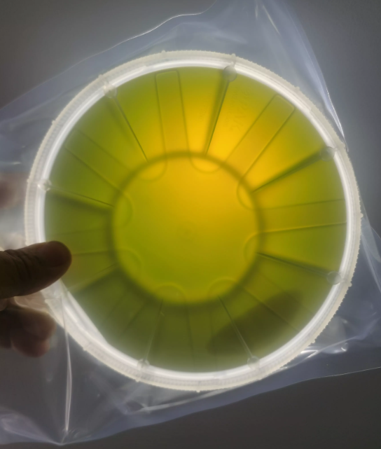
6 inch wafer
6 inch wafer :Silicon carbide, also known as carborundum, is a semiconductor electronic device with silicon river beach chemical formula for this orchid turtle back to work under high temperature or high pressure, or both. Silicon carbide is also one of the important LED components. It is the most commonly used substrate during the growth period, and it also rushes into the diffuser in the high-power LED. Our customized sizes range from 2 inches, 3 inches, 4 inches, 6 inches, high-purity 4H-N4 inches, 6 inches diameter 150 mm, silicon carbide, single crystal (sic) substrates wafers.
6 inch wafer
Free Standing gan Wafer | Single Crystal Substrates
Si Doped Undoped Laser Device Gallium Nitride Wafer
300mm Gan Wafer | Gallium Nitride Wafer For Power Micro LED
8 Inch 12 Inch 6Inch gan Wafer
2 Inch 4 Inch GaN Wafer | Gallium Nitride Wafer
4inch 6inch GaN-ON-SiC EPI layer
6 inch wafer
What is a 6 inch wafer?
6 inch wafer :silicon wafer is a kind of wafer manufactured by photolithography, which is a kind of equipment used for IC manufacturing, and a nuclear material.
At present, it has become one of the most commonly used and widely used substrates in the semiconductor industry.
Its smooth and polished surface makes it a perfect choice for many microelectronic devices. These chips provide power for most electronic devices on the market, and they are also excellent raw materials in integrated circuits.
The main advantage of using silicon in integrated circuits is that it has excellent high purity, which can make the surface of the wafer polished to be as smooth as a mirror, so that it is easier to print the circuit layout.
At present, it is the second abundant raw material in the world. It is a natural mineral, and then slowly grows into a large crystal.
The crystal is buffered to remove impurities and cut into thin sheets. The resulting wafer can be cut into any shape and size, which makes it possible for silicon chips to be used in many different applications. The reason why silicon chips are used in integrated circuits is that their cost is relatively low. Compared with other raw materials, manufacturers can reduce the processing time of the circuits they produce, Therefore, the cost of manufacturing a new generation of products can be more effectively controlled. Cost of drugs.
There are two main types of silicon wafers. First, the 4-inch diameter gold dollar, which is the standardized essence used in most electronic devices. The other type is the 6-inch diameter ghost chip that we mainly mentioned today. Although these are thinner than the 4-inch ones, they also have obvious effects in terms of production efficiency. In order to achieve the best performance, it is more important to have a strong and solid gold source, There are several different wafer shapes to choose from, such as rectangle, square, and circle. Hexagonal For all these options, we can also customize the wafer shape you need.
If you are in the semiconductor industry, you may want to know how important it is to choose the right direction for silicon chips. The right direction is very important for the effective production and maximum output of semiconductors. It is not always easy for him to decide what is the best choice. The following are some considerations when you make a decision.
First of all, it has many common things about different types of silicon wafers, oriented wafers. When these wafers are knocked, they are divided into several pieces. They are easier to split than silicon wafers in other crystal directions.
Another kind of silicon chip is easier to be split, which is easier to be used for chip manufacturing.
One of the most useful advantages of Guiping is its heat dissipation performance. In applications requiring high temperature, Pingtan silicon chip is a popular choice. It usually has a black stripe, which can prevent the heat on the surface from transferring to the interior of the component.