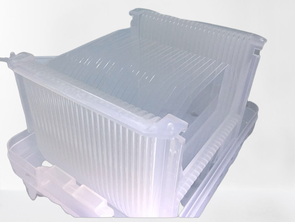
8 Inch 12 Inch 6 Inch Gan Wafer
8 Inch 12 Inch 6 Inch Gan Wafer : We are committed to offering premium GaN epi wafers for use in RF, micro-LED, and power electronic applications.

8 Inch 12 Inch 6 Inch Gan Wafer
8″ 12″ 6″ GaN-On-Si EPI-WAFERS For Power RF LED Applications
Wafer epitaxial for GaN (GaN EPI on Silicon)
China is a supplier of GaN-on-Si epitaxial wafers. Gallium nitride (GaN) is widely employed in power devices and blue light-emitting diodes due to its large energy gap.
Introduction to the 8-inch, 12-inch, and 6-inch Sapphire Wafer
Improving information and communication technology and conserving energy are becoming increasingly crucial. Gallium nitride (GaN), the next-generation semiconductor material, was employed to construct a semiconductor substrate with a large bandgap in order to meet these specifications.
By developing single-crystal GaN thin films on silicon substrates, we produce humongous, low-cost semiconductor substrates for next-generation devices.
.
The main targets for household appliances are switchgears and inverters with hundreds of failure voltages. Mobile phone base stations utilize transistors with high power and high frequency.
Our silicon substrates are less expensive to produce GaN on than silicon carbide or sapphire substrates, allowing us to deliver GaN devices tailored to the needs of our customers.
The energy field formed by the band structure in an electron-free crystal is known as the band gap (semiconductor materials with a band gap larger than silicon are often referred to as wide band gap semiconductors). Material with a large bandgap, a high electrical breakdown voltage, and good optical transmittance
Heterojunction is a mixture of several substances. In the semiconductor field, relatively thin layers of semiconductor materials with varied compositions are often stacked. Mixed crystals provide heterojunctions with atomically smooth surfaces and advantageous interface characteristics. These interactions culminate in the development of a layer of highly mobile two-dimensional electron gas.
8-by-12-by-6-inch Sapphire Wafer
Specs for blue GaN-on-Si LED Epi-wafer
Our objective is to produce GaN LED epi wafers on Si substrates in diameters ranging from 100 mm to 200 mm. The wafer quality meets the following criteria:
8-by-12-by-6-inch Sapphire Wafer
• The core technical team members all have more than ten years of GaN capacity experience.
• 200k units per year for 150mm GaN epiwafers in a 3,300 square meter class 1000 cleanroom Product s Diversity
• GaN-on-HR Si (up to 150mm); • GaN-on-SiC (up to 300mm); (up to 200mm)
• GaN-on-GaN (up to 150 mm); GaN-on-Sapphire
8 Inch 12 Inch 6 Inch Gan Wafer
When you want to look for 2 double side polished sapphire wafer, if you will search those keywords to found us ? Such as 2 inch sapphire wafer,2 inch sapphire wafer price,2 inch sapphire wafer thickness,2 sapphire wafer, double-side polish 2 sapphire wafer etc ?