Sapphire Single Crystal Substrate & Wafer
Sapphire Single Crystal Substrate : XKH sapphire wafers have a wide range of applications, and our sapphire substrates can be used for growth of III-V compounds such as GaN for LED’s, The types include A-Plane sapphire substrates, C-Plane substrates and R-Plane substrates. In short, they are all the preferred raw materials for the deposition of silicon used in microelectronics. XKH, welcome to inquire about our products and prices. We are willing to provide you with strong after-sales service.
Sapphire Single Crystal Substrate & Wafer
Free Standing gan Wafer | Single Crystal Substrates
Si Doped Undoped Laser Device Gallium Nitride Wafer
300mm Gan Wafer | Gallium Nitride Wafer For Power Micro LED
8 Inch 12 Inch 6Inch gan Wafer
2 Inch 4 Inch GaN Wafer | Gallium Nitride Wafer
4inch 6inch GaN-ON-SiC EPI layer
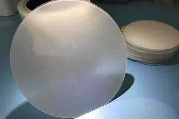
Sapphire Single Crystal Substrate & Wafer
Sapphire Single Crystal Substrate : The double sided polished Sapphire Substrate made in China covers both the C plane.Its dimensions include 4 inches, 6 inches, 8 inches, and some special sizes. We can also provide customized services.The surface is treated by a DSP or SSP.Mainly used in semiconductor carriers or some optical applications. The main material for sapphire wafer is high purity single crystals Al2O3. The thickness is basically 1300 +/- 25 um.Its Bow and warp are all smaller than 25 microns.The C plane is basically maintained within (0001) off M (1-100) plane 0.2 +/- 0.05 degree. The packaging we use is a vacuum sealed container filled with nitrogen gas in a Class 100 environment, which is non polluting. Polishing can be done on one or both sides.The reverse side of SSP wafer was fine ground to Ra = 0.8 – 1.2 um. The raw materials we choose are of high quality, with sapphire crystal oriented along the c-axis and a thickness of 0.725 millimeters. They are used in semiconductor display boards and optics, and the SS and PS decolorization rates have reached 85%. There are many sizes available for you.