8 inch wafer
8 inch wafer: If you need 8-inch silicon wafers, we can provide them to you. According to your different thickness requirements and quantity requirements, we will do our best to meet your needs. We also provide 12 inch 2-inch 4-inch 6-inch wafers. Please contact us now, and we will recommend the most high-quality 8-inch wafers to you.
8 inch wafer
Free Standing gan Wafer | Single Crystal Substrates
Si Doped Undoped Laser Device Gallium Nitride Wafer
300mm Gan Wafer | Gallium Nitride Wafer For Power Micro LED
8 Inch 12 Inch 6Inch gan Wafer
2 Inch 4 Inch GaN Wafer | Gallium Nitride Wafer
4inch 6inch GaN-ON-SiC EPI layer
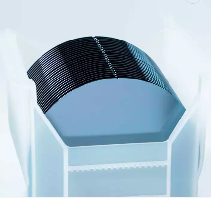
8 inch wafer
What You Need to Know About an 8 inch wafer? If you plan to buy an 8-inch wafer, you need to understand the different problems caused by using this chip. The size of the wafer has a lot to do with its strength and the output you get there. The 8 inch wafer chip strength at the edge of the wafer is higher than the internal part.Generally, a semiconductor wafer is a multi-layer structure, which is composed of a semiconductor layer, an insulating layer and a top shielding layer. These cities are separated by a channel and multiple channels, and are packaged with protective materials. The bottom line is the other half of the gold source, which is called silicon substrate. The semiconductor layer has a crystal structure similar to the semiconductor substrate. It has several columns with different conductivity types. Various metal interconnections also form rock and soil in the village to form various climaxes. Their depth is about 5~40mm. In the next few years, the global production demand for 8-inch wafers will still be very, very large, and will continue at a growth rate, which is an important development for the semiconductor manufacturing sector. In general, if the silicon material is too thin to be effectively kneaded and the wafers generation, one solution is to create an offset grid on the substrate to improve the layout of the silicon products. Compared with 12 inch wafers, the cost of an 8 inch wafer is much higher. In order to meet customers’ requirements for 8-inch wafers, we are constantly improving our process capability to produce wafers in a high-speed and high-quality way.