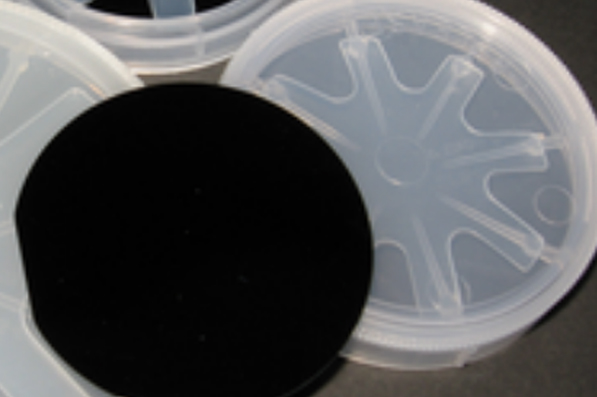
al2o3 wafer | al2o3 si wafer r-plane & C-plane in China
al2o3 wafer r-plane and C-plane are relatively conventional type.Due to its stable chemical and physical properties, it has become one of the best substrate materials for superconductors and magnetic epitaxial films, as well as a raw material for III-V nitrides.

Sapphire Wafer
2 Inch A - Axis Sapphire Wafer For EPI
5 Inch Sapphire Wafer R Plane Dia 125mm
8 Inch Sapphire Wafer Dia 200 mm
Sapphire Al2O3 Wafer
12 Inch Sapphire Wafers Dia 300mm
4 inch Sapphire Wafer C-Plane Single or Double Side Polish Al2O3 Single Crystal
6 inch Sapphire Wafer C-Plane Single or Double Side Polish Al2O3 Single Crystal
3 inch Sapphire Wafer C-Plane Single or Double Side
al2o3 wafer
This is just a chemical formula. In principle, it is a transparent-colored sapphire raw material. Its mechanical properties and strength, as well as the thermal and corrosion resistance properties of desk lamps, have become one of the best raw materials in the semiconductor industry.
All of our wafer ingots are made of highly pure single crystal materials | Al2O3, which are a type of sapphire chip.
In terms of packaging, we chose the packaging method of cardboard boxes and cardboard boxes, and used vacuum sealed containers filled with nitrogen gas in the environment for packaging.
This packaging can prevent contamination of our sapphire wafer.
For polishing, we choose single sided and double sided polishing, and of course, we can also provide you with unpolished sapphire lenses.
The clarity of single sided polished gold elements on the back can be polished to between 0.8 and 1.26 um.
Our thickness change is basically controlled within a range of less than 20 um, And the warp and Bow that everyone is most concerned about are less than 25 micrometers, respectively.
al2o3 wafer ,There are c plane and m plane in the direction.The length of the plane is basically 17.5 millimeters, with an error of ± 1mm.
The production steps of our sapphire wafer al2o3 wafer are basically divided into the following parts:
The first step is to choose a sapphire crystal body,This step is very crucial because if the first step is not rigorous when selecting this raw material, it will directly affect the quality of the final product.
Therefore, when choosing sapphire crystal, We need special rigor.And this step is also the most basic step of the standardized production concept that our factory has always emphasized.
Customize the ingot axis, This is our second step in producing sapphire this year.Then we will cut off the tail and top.Then we will modify the shape of its diameter.
Next, we will proceed with grinding, which is the so-called surface grinding step. We can choose either single-sided grinding or double-sided coating according to the customer’s requirements.
After annealing, we will perform wire cutting. Chamfering is in progress.Return it again, grind it, and then polish it.The final step is infection. We will simply divide them into several steps and provide a brief description.
Produce step for saphire wafers
Sapphire crystal body—>get rough ingot in customized axis—>cut tail& top off—->
repair diameter shape—-> Grind OF surface—>( anneal –>)wire cut—>chamfer–>anneal—>lapped—polished—infection
We hope to have a better understanding of our sapphire for you