Semiconductor silicon wafer
Semiconductor silicon wafer :Silicon is one of the most commonly used semiconductor materials. It is widely used in computer chip photovoltaic, electronic lasers, liquid crystal displays and transistors. It is also an important part of the power electronics industry. Silicon chip is a thin piece of high-purity crystalline silicon.
Semiconductor silicon wafer
Free Standing gan Wafer | Single Crystal Substrates
Si Doped Undoped Laser Device Gallium Nitride Wafer
300mm Gan Wafer | Gallium Nitride Wafer For Power Micro LED
8 Inch 12 Inch 6Inch gan Wafer
2 Inch 4 Inch GaN Wafer | Gallium Nitride Wafer
4inch 6inch GaN-ON-SiC EPI layer
Semiconductor silicon wafer
Semiconductor silicon wafer:
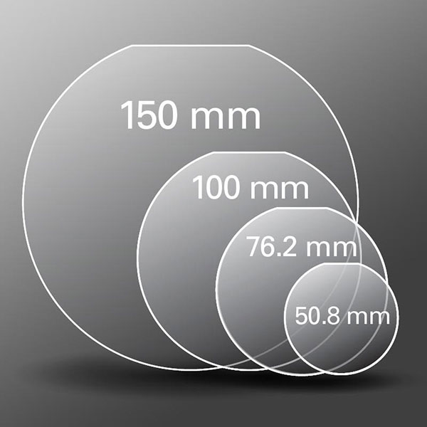
We provide wafers with diameters ranging from 2 inches to 8 inches. The surface quality is better than 40 / 20. Its raw material is silica gel, with a thickness tolerance of ± 0.1mm and a dimension tolerance of 0.1mm.
We focus on the design and batch manufacturing of high-performance wafer products, which can be used in optical components, such as lenses, near window filters, static optical instruments and laser systems, as well as military, telecommunications, medical and environmental monitoring industries. The materials range from optical glass to infrared and ultraviolet glass.As a rapidly developing optical supplier, we provide high-quality services and products.
Our products have been sold to Europe and America, and we have established long-term cooperative relations. Our advanced technology and quality control have rapidly helped our customers and improved the reputation of our products.
Silicon wafer is an efficient semiconductor material, which can be used in a wide range of voltage, its crystal structure and many dopants, making it an ideal choice for controlling resistance, thermoelectric stability and other characteristics.
However, the cost of raw materials is sometimes unstable, which may be one of the obstacles to the development of semiconductor silicon wafer market.