Germanium wafer
Germanium wafer : Ge wafer is an elemental and common semiconductor material that is widely employed in sensor, solar cell, and infrared optics applications due to its good crystallographic characteristics and unique electric properties. To fulfill your specific germanium requirements, we can deliver low dislocation and epi ready Ge wafers.
Germanium wafer
Free Standing gan Wafer | Single Crystal Substrates
Si Doped Undoped Laser Device Gallium Nitride Wafer
300mm Gan Wafer | Gallium Nitride Wafer For Power Micro LED
8 Inch 12 Inch 6Inch gan Wafer
2 Inch 4 Inch GaN Wafer | Gallium Nitride Wafer
4inch 6inch GaN-ON-SiC EPI layer
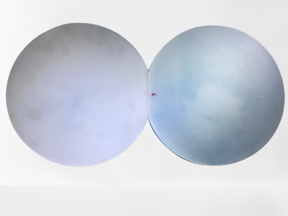
Germanium wafer
Germanium wafer The semiconductors used in photovoltaics are often produced using Germanium wafers. It is extremely fragile and sensitive. It is produced by a procedure called chemical vapor deposition. It expands when frozen and is incredibly pure. As a result, it is particularly well-liked by the makers of photovoltaics. greater purity than germanium Germanium is a valuable material due to its various qualities in addition to its electrical conductivity. It is an excellent material for semiconductor devices because of these qualities. Additionally, it is simple to include into the silicon chip production process. In high-power devices, it is also less likely to deteriorate. It is a promising contender for light-powered computer chips because of this. Germanium and silicon are the two most popular materials used in the semiconductor industry. Both have many different applications. However, due to its lower cost and higher purity, silicon is more suitable for consumer devices. Compared to germanium, it is also simpler to process. Germanium wafer Germanium has a low density, making it a useful material for semiconductor devices. It melts at a higher temperature than silicon. Additionally, it is moveable. In some situations, it can also be utilized as a silicon alternative. It is also an excellent material for optical computing. In nature, germanium can be found as an oxide or sulfide. It is frequently present in copper and zinc ores as a partner. Additionally, it can be made into oxide rods, granules, or powders. It is a rather uncommon element. Online stores are the greatest place to get semiconductor materials. It is wise to evaluate prices before making a purchase because prices can change drastically. Additionally, you can learn more about costs by reading industry news. Parallel partial secondary dislocations form a dislocation grid in germanium bicrystals. They also display networks of interfacial dislocations and stacking fault-like structures. Germanium wafer When it becomes cold, it expands. Different semi-conductor materials offer unique qualities and benefits. It’s crucial to be aware of the materials’ costs and availability. You may want to look at the costs of some internet sources for semiconductor materials. The quantity you need to purchase will have a significant impact on the price of semiconductor materials. There’s no need to spend a fortune if you’re seeking for a high-purity substance. Silicon is one of the most popular types of semiconductor materials utilized in semiconductor devices. When frozen, the solid silicon expands like water but does not chemically react with oxygen. It is a suitable option for consumer electronics because of this. However, some electrical applications cannot use it due to its inferior electrical conductivity. A semiconductor material that expands when frozen is germanium, another type of semiconductor material. This is due to the material’s high melting point as a semiconductor. SiO2, a different kind of semiconductor material, doesn’t expand as much when frozen as other semiconductor materials. The SiO2 substance, however, is more appropriate for electronic applications like computer chips. Germanium wafer The best place to find out the cost of a semiconductor material is to contact a trustworthy business that prioritizes quality. The internet is your friend, though, if you’re seeking for a quick and simple way to find out how much a semiconductor material costs. The most recent prices can be found by reading industry news. To see whether you can find a better deal, you can also use price comparison websites. The most crucial thing to note is that it can be challenging to locate semiconductor materials. However, if you’re wanting to produce semiconductors, you’ll want to locate premium materials that are inexpensive and simple to work with.