silicon substrate manufacturer & Supplier in China
silicon substrate is a kind of material used in many applications, including optics. This material is made of silicon. It is a semiconductor industrial material. For various reasons, it has good conductivity, corrosion resistance and molding ability. There are various processes for manufacturing silicon wafers | XKH silicon substrate.
silicon wafer buy from China
8 Inch 12 Inch 6Inch gan Wafer
2 Inch 4 Inch GaN Wafer | Gallium Nitride Wafer
4inch 6inch GaN-ON-SiC EPI layer
silicon substrate | Professional manufacturer & Supplier in China
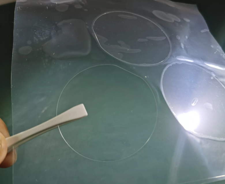
We offer different silicon substrate thickness at the same time.In the process of making silicon wafers, Many complicated steps are involved,
These tasks are carried out in an appropriate way to ensure that the level of our silicon wafer and the ability required for its execution can be completely ensured.
If these steps are not carried out in a strict way, the silicon wafer will be contaminated and may even lead to the failure of the semiconductor equipment.
In all the steps, we particularly emphasize that the silicon substrate should be cleaned after slicing.
Your purpose of removing pollution is to use chemical and mechanical polishing processes to remove microcracks, scratches and surface layers. These are very critical steps.
Use special mats to remove the micro-dust of silicon wafers.
The silicon wafers that pass the inspection are then packaged in vacuum-sealed plastic bags for storage to ensure that they are not contaminated.
In fact, polishing the silicon wafer during all the manufacturing process is extremely important for the state of its surface.
In this process, a special polishing shop is applied to the surface of the gold source to remove any defects and produce a mirror effect.
In this case, a thick oxide layer is also applied to the surface of the gold source to provide isolation from the metal wiring layer.
We use chemical abrasives that are finely dispersed alumina or silica to grind into particles or into hard polyurethane polishing pads.
We all know that silicon wafers play an important role in the whole optical field. Its application range is extremely wide, Is widely used in various devices, These devices, including optical fiber and infrared sensors, are also commonly used in video originals and power components。
In addition, it is also used in miniature optical instruments as a specific semiconductor material, which is mainly used in electronic devices, and also has applications in optical systems such as anti-color optics.
The structure consists of a thin layer of monocrystalline silicon, which is usually combined with a layer of silicon oxide, which is two microns thick.
In order to increase the diameter of silicon substrate, we added a lot of raw materials. At the same time, we need to pay special attention to the smoothness of inspectors.
In addition, the finished silicon substrate must be able to support the key points. Therefore, we specially developed some specific processes to achieve this requirement.
Usually, the shape of the silicon wafer we see is round, and the shape of the edge is to remove sharp edges. When the silicon wafer is cut, the two ends are often sharpened, and these edges help to reduce the risk of sliding. These are the four main purposes.