Gan Substrate
Gan Substrate : Our gallium nitride substrate is manufactured using advanced processes and methods and wafer processing technology. This technology has been accepted by customers for many years. Its characteristics are good uniformity, smooth surface quality and high cleanliness, that is, the advantage of purity is particularly obvious. This high-quality single crystal substrate, that is, gallium nitride wafer, is widely used in electronic products.
Gan Substrate
8 Inch 12 Inch 6Inch gan Wafer
2 Inch 4 Inch GaN Wafer | Gallium Nitride Wafer
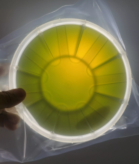
4inch 6inch GaN-ON-SiC EPI layer
Si Doped Undoped Laser Device Gallium Nitride Wafer
300mm Gan Wafer | Gallium Nitride Wafer For Power Micro LED
Your Best Gan Substrate Partner in China | Gan Wafer
GaN wafers, is also called gallium nitride wafer. It is a unique semiconductor material and plays a very important role in various applications.
Gan Substrate is famous for its high-end music, high electron mobility and broadband system, which makes it one of the important raw materials for high-power and high-frequency electronic equipment.
The production of high power and high frequency transistors is one of the most common applications of GaN chips.
These transistors are used in various amplifiers, radios and mobile phones, that is, in some electronic devices.
Gan Substrate can work at a much higher frequency than traditional silicon transistors, which is why they play a highly efficient role in high-speed communication systems.
When our potassium nitride chips | Gan Substrate are used to produce light-emitting diodes, that is, some LED clocks, their brightness will produce better efficiency.
These LEDs have high efficiency, and their life is much longer than traditional incandescent lamps. Therefore, they have become popular raw materials for various lighting purposes.
GaN based LEDs can also produce a wider range of colors than traditional LEDs.Make them become the unique selected RAW materials in some application fields with relatively high requirements and sensitive requirements for color.
Of course, in addition to the transistor and LED applications, they are also used to produce high-performance solar cells and high electronic products. They are also explored for various other applications, including the production of sensors, transistors and even medical devices.
That is to say, because the unique performance of GaN wafers is extremely broad in applications, we will not give examples here.In the next few years, they will become the raw materials with large demand in the electronic industry and photoelectric industry.
LED Gan Wafer , If you need to find suppliers and manufacturers of gallium nitride wafers, or even customized requirements with special requirements, you can contact us. We have rich experience in these areas, including Sapphire wafer or Silicon carbide wafers, including Potassium nitride gold source, Please contact us now.