double side polished silicon wafers Supplier & Manufacturer
Double side polished silicon wafers, We can provide not only double sided polishing, but also single sided polishing or non polishing silicon carbide wafers.
Silicon carbide crystal, also known as silicon carbide, is a semiconductor with two elements of silicon and carbon.
Its chemical formula is sic. Silicon carbide has good stability under high temperature or high pressure, and it is mainly used in semiconductor electronic equipment.
It is also an important component for LED products. It is a common substrate for growing roots. It can also be used as a radiator power supply under high voltage.
2 Inch A - Axis Sapphire Wafer For EPI
5 Inch Sapphire Wafer R Plane Dia 125mm
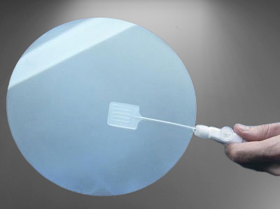
8 Inch Sapphire Wafer Dia 200 mm
Double Side Polished (DSP) Silicon Wafers
12 Inch Sapphire Wafers Dia 300mm
4 inch Sapphire Wafer C-Plane Single or Double Side Polish Al2O3 Single Crystal
6 inch Sapphire Wafer C-Plane Single or Double Side Polish Al2O3 Single Crystal
Double Side Polish Silicon Carbide Wafer 2-6'' 4H N - Doped SiC Wafers
Double side polished silicon wafers
If you require double-sided polishing, we can provide this service and product.Generally, we carry out single-sided polishing or double-sided polishing or even non-polishing according to the specific requirements of customers, all of which depend on the needs of customers.
double side polished silicon wafers
“We provide our users with hyperplane double–ided polishing of various diameters, thickness directions, and electrical resistivity. Our inventory is available from different thicknesses.
In order to improve the flatness of the silicon wafer, that is, to polish the back surface of the silicon wafer, we generally recommend that users use double sided polishing, as it will help reduce the roughness of the surface of the silicon wafer.”.
When remanufacturing equipment requiring ultra plat and ultra low roughness specifications. Double sided polishing is necessary.
Product | 4H-SiC | |||
Grade | Grade I | Grade II | Grade III | |
polycrystalline areas | None permitted | None permitted | <5% | |
polytype areas | None permitted | ≤20% | 20% ~ 50% | |
Micropipe Density) | < 5micropipes/cm-2 | < 30micropipes/cm-2 | <100micropipes/cm-2 | |
Total usable area | >95% | >80% | N/A | |
Diameter | 100.0 mm +0/-0.5 mm | |||
Thickness | 500 μm ± 25 μm or Customer Specification | |||
Dopant | n type: nitrogen | |||
Primary Flat Orientation) | Perpendicular to <11-20> ± 5.0° | |||
Primary Flat Length | 32.5 mm ± 2.0 mm | |||
Secondary Flat Orientation) | 90° CW from Primary flat ± 5.0° | |||
Secondary Flat Length) | 18.0 mm ± 2.0 mm | |||
On axis Wafer Orientation) | {0001} ± 0.25° | |||
Off axis Wafer Orientation | 4.0° toward <11-20> ± 0.5° or Customer Specification | |||
TTV/BOW/Warp | < 5μm / <10μm /< 20μm | |||
Resistivity | 0.01~0.03 Ω×cm | |||
Surface Finish | C Face polish.Si Face CMP (Si face: Rq < 0.15 nm) or Customer Specification | Double side polish | ||
Double side polished silicon wafers
Main advantages and characteristics.
- The density is indeed depressed.
- High quality crystal.
- It can be used to improve the scale of semiconductor manufacturing.
- The tolerance range applicable to some specific equipment manufacturing requirements.
- It can optimize the performance and cost control of power electronic equipment.
To produce high quality 200 mm silicon carbide wafers is a way for us to provide quality assurance for many users. Whether it is 150 mm to 200 mm, we can provide stable quality and high performance quality.
The use of silicon carbide wafers is actually very extensive. It is mainly used to manufacture high voltage and high power atomic devices, such as diodes, power transistors and high power microwave devices, and so on.
We can list them in detail in the next article about double side polished silicon wafers.
If you just need 200mm sic wafers , please contact us immediately.