gap substrate |GaP Wafer,Gallium Phosphide Wafer
Gap substrate is also known as GaP Wafer,GaP Substrate,Gallium Phosphide Wafer. The material grown on the Gap crystal substrate by liquid phase epitaxy or vapor phase epitaxy diffusion is the Gap substrate material, which is mainly used for some traffic light yellow light diodes, or is widely used in some light-emitting diodes.GaP Wafer vapor phase epitaxy diffusion, production materials can produce yellow chartreuse light-emitting diodes.
2 Inch A - Axis Sapphire Wafer For EPI
5 Inch Sapphire Wafer R Plane Dia 125mm
8 Inch Sapphire Wafer Dia 200 mm
Gap substrate | Gallium Phosphide (GaP)
12 Inch Sapphire Wafers Dia 300mm
4 inch Sapphire Wafer C-Plane Single or Double Side Polish Al2O3 Single Crystal
6 inch Sapphire Wafer C-Plane Single or Double Side Polish Al2O3 Single Crystal
GaP substrate | Gallium phosphide wafer Supplier
Gallium Phosphide(GaP) epitaxial material is mainly used in laser diodes and some semiconductor materials, as well as some light-emitting LED lamps. Its high quality helps these electronic products.
In some environments that need to withstand high temperatures, it can also show extremely strong stability, especially its thermal conductivity and chemical stability are particularly prominent.
So if your application field has great requirements for high temperatures, So choosing our GaP substrate product is the right choice.
One advantage of it is its lower cost-effectiveness.
Compared with other sapphire-related materials, its economic benefits are more significant, as its cost is lower, which greatly enhances the competitiveness of equipment grown on AP.
Our information is basically polished and cleaned with advanced equipment, which is guaranteed to have better quality with higher cleanliness.
Our GaP substrate can only be controlled to the maximum extent, and material defects can help reduce the absorption of light by sapphire.
Main advantages and characteristics.
- The density is indeed depressed.
- High quality crystal.
- It can be used to improve the scale of semiconductor manufacturing.
- The tolerance range applicable to some specific equipment manufacturing requirements.
- It can optimize the performance and cost control of power electronic equipment.
Advancement
• Low lattice mismatch
• High thermal conductivity
• Low power consumption
• Excellent transient characteristics
• High band gap
Property | 4H-SiC, Single Crystal | 6H-SiC, Single Crystal |
Lattice Parameters | a=3.076 Å c=10.053 Å | a=3.073 Å c=15.117 Å |
Stacking Sequence | ABCB | ABCACB |
Mohs Hardness | ≈9.2 | ≈9.2 |
Density | 3.21 g/cm3 | 3.21 g/cm3 |
Therm. Expansion Coefficient | 4-5×10⁻⁶/K | 4-5×10⁻⁶/K |
Refraction Index @750nm | no = 2.61 ne = 2.66 | no = 2.60 ne = 2.65 |
Dielectric Constant | c~9.66 | c~9.66 |
Thermal Conductivity (N-type, 0.02 ohm.cm) | a~4.2 W/cm·K@298K c~3.7 W/cm·K@298K | |
Thermal Conductivity (Semi-insulating) | a~4.9 W/cm·K@298K c~3.9 W/cm·K@298K | a~4.6 W/cm·K@298K c~3.2 W/cm·K@298K |
Band-gap | 3.23 eV | 3.02 eV |
Break-Down Electrical Field | 3-5×10⁶V/cm | 3-5×10⁶V/cm |
Saturation Drift Velocity | 2.0×10⁵m/s | 2.0×10⁵m/s |
This way, when GaP substrate is applied to LED production, the efficiency of LED will be greatly improved.
After using the wafer substrate produced by Xinkehui, it can greatly improve the excellent quality of Gap substrate .
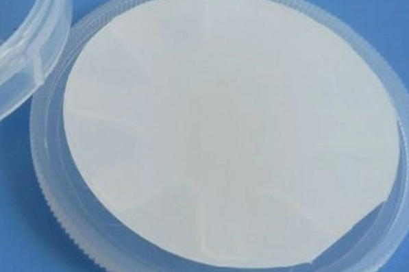
It is used as a carrier for wafer bonding ,We have a wide variety of products, including 2 inches, 3 inches, 4 inches, 6 inches, 8 inches, and 12 inches in standard sizes. For some other special sizes, we can also provide customized services.
We look forward to your inquiry and establish a reliable long-term cooperative relationship.