Semi conductor wafers
Semi conductor wafers: A wafer is a thin slice of semiconductor crystal with essentially identical physical and electrical properties to its mother substance, the crystalline semiconductor, but is used as the foundation for a variety of electrical, electronic, and microelectronic devices and tools.
Semi conductor wafers
Free Standing gan Wafer | Single Crystal Substrates
Si Doped Undoped Laser Device Gallium Nitride Wafer
300mm Gan Wafer | Gallium Nitride Wafer For Power Micro LED
8 Inch 12 Inch 6Inch gan Wafer
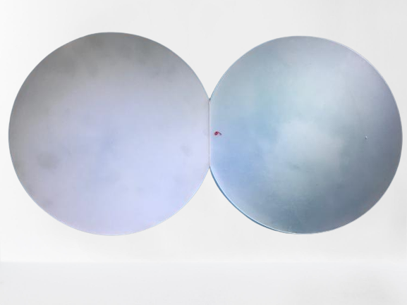
2 Inch 4 Inch GaN Wafer | Gallium Nitride Wafer
4inch 6inch GaN-ON-SiC EPI layer
Semi conductor wafers
Semi conductor wafers
The semiconductor business uses a variety of semiconductor types. These include filament evaporation, organic, germanium, extrinsic, and semiconductors. While other semiconductors are utilized in electrical devices, some are employed in semiconductor production machinery.
semiconductors that are external :Semi conductor wafers
Semiconductor wafers are employed in the creation of microchips and integrated circuits, among several other applications. Additionally, they assist in the calibration of numerous devices. Gallium arsenide or silicon can be used to make the wafers.
The most used wafer material is silicon. Additionally, it is employed in the production of diodes, integrated circuits, and transistors. However, silicon has a low conductivity and performs poorly as an electrical conductor. The idea of doping was created to solve this issue. The electrical characteristics of the material are altered via doping. Impurities are added to the substance during doping. Typically trivalent or pentavalent, these impurities. The conductivity of a material can vary depending on its characteristics and the quantity of doping atoms.
To alter the electrical characteristics of a semiconductor, an atom or molecule known as a dopant is added. Sulfur, metals, and ions are dopants. Ion implantation or photolithography are two methods for boosting the concentration of the dopants. Diffusion can also increase the number of doping atoms.
The density of the charge carriers is influenced by the quantity of doping atoms. The quantity of charge carriers affects the material’s electrical conductivity. When the dopant concentration is low, the material’s electrical conductivity will also be poor. On the other hand, heavily doped materials will behave more like conductors.
Dopant atoms can move through the crystal like positively charged particles when they are put into the semiconductor. The density of the electrons and holes changes as the dopant atoms enter the semiconductor.
The dopant atoms may be added at the beginning or later stages of the growth of the semiconductor crystal. Vapor phase epitaxy can be used to dope materials as well. In this procedure, a layer of silicon crystal is applied to the material in order to add the dopant atoms. On a substrate made of silicon carbide, these layers are then formed.
Semi conductor wafers
Extrinsic semiconductors are doped with impurities and are semiconductors. They are frequently utilized in semiconductor lasers, lasers, and light emitting diodes (LEDs). Extrinsic semiconductors’ electrical conductivity is influenced by the quantity and concentration of dopant atoms.
Natural semiconductors
Organic semiconductors are produced by a number of intricate techniques. It necessitates the use of modifiable processing factors, such as the substrate and solution temperatures. The creation of procedures that make use of less hazardous solvents can lead to the solution and substrate being in their ideal state.
Advanced solution techniques are now making progress for printing single-crystal thin films in addition to the conventional methods for amorphous thin films. These methods show promise for printing single-crystal thin films across huge areas.
Single crystals of two-dimensional organic semiconductors are a desirable class of materials for advanced electronic devices. These materials have excellent electronic characteristics and can be produced at modest temperatures. Additionally, they show hardly any flaws and have strong charge carrier mobilities. These materials are also appropriate for uses like organic p-n heterojunction devices and flexible strain sensors.
Semi conductor wafers
Because of improvements in chemical synthesis and a better knowledge of the charged states of organic materials, the study of organic doping has grown in recent years. Recent research has demonstrated that these materials’ processability can be impacted by their shape. Theoretical prediction is still difficult, though. Furthermore, it is still unknown how the crystal structure of organic semiconductors relates to their characteristics. Nevertheless, these scientific advances imply that the importance of molecular doping in fabrication.
Semi conductor wafers
The crystal structures of these materials had a significant role in determining their processability in the early stages of development. X-ray diffraction crystal structures served as the foundation for many theoretical research. Recent research has, however, concentrated on comprehending the molecular dynamics and structure of these materials. Recent improvements in crystal structure prediction for p-type organic semiconductors have been made as a result of these discoveries.