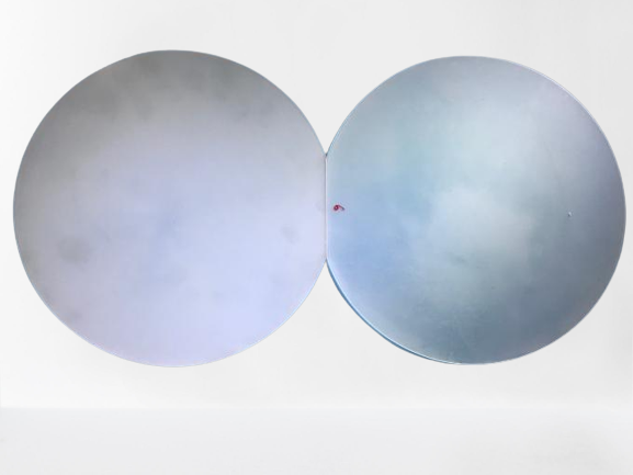
Silica wafer
Silica wafer : A silicon wafer is a necessary component for the production of semiconductors, which are used in a variety of electrical products that enhance our lives. Few of us meet genuine silicon wafers in our everyday lives.
Silica wafer
Free Standing gan Wafer | Single Crystal Substrates
Si Doped Undoped Laser Device Gallium Nitride Wafer
300mm Gan Wafer | Gallium Nitride Wafer For Power Micro LED
8 Inch 12 Inch 6Inch gan Wafer
2 Inch 4 Inch GaN Wafer | Gallium Nitride Wafer
4inch 6inch GaN-ON-SiC EPI layer
Silica wafer
Silica Wafer Applications
The silicon wafer can be used in a variety of ways. These include applications for semiconductor, optical, and electronic devices as well as bonding of two or more micro components.
the procedures used to produce them
The creation of silicon wafers involves thousands of steps in the manufacturing of semiconductor devices. These procedures result in gadgets with certain functional behaviors.
Growing an ingot is the initial step in creating a silicon wafer. In an electric furnace, silica and carbon are heated throughout this process. The silicon is cleaned in this manner. Depending on the size and quality of the ingot, the growing process can take anywhere from a week to a month.
Chemical cleansing is the second step. This procedure eliminates minute impurities and flaws. The majority of the time, sodium hydroxide is used for this.
The subsequent step in creating a silicon wafer is polishing. To reduce the amount of dust and other contaminants on the wafer’s surface, this is carried out in a clean room. Maintaining cleanliness at the desk is also crucial.
Typically, there are two or three phases to the polishing process. The surface is polished using colloidal silica, a unique abrasive.
In a clean room, the polishing procedure is also carried out. In order to remove any extra particles, the procedure is also carried out with a fan present.
Additionally, the silicon wafer is polished to facilitate use. The wafer can be printed with circuit design thanks to its smooth surface.
The final step in creating a silicon wafer necessitates extensive polishing and cleaning. To reduce the amount of dust and other debris on its surface, this is carried out in a spotless environment.
Silica wafer
A thin piece of crystalline silicon called a silicon wafer is utilized in the production of microelectronic devices. The most popular substrate for semiconductor devices is the silicon wafer. Microelectronics and solar cells are only a couple of the technologies that use silicon wafers.
Applications for optics
Reflective optics, optical fibers, and infrared applications all make use of silica wafer in optical applications. In these situations, the surface is treated to reduce surface stress and strain.
Fluorescence studies were used to examine the functionalized silicon wafer’s optical characteristics.
applications for semiconductors Silica wafer
A silicon wafer is essentially a tiny piece of crystal semiconductor. It serves as the foundation for many different technological gadgets. One of these is an integrated circuit. The best semiconductor, silicon, is used to create microelectronic devices.
The second most common element in the crust of the planet is silicon. It makes up roughly 26% of the crust. The pure form required for electrical applications is not naturally generated. This is obtained by purifying silicon from quartz sand.
Microelectronic device construction also uses silicon wafers. One example of them is an integrated circuit, which has millions of transistors, capacitors, and resistors. For electronic equipment to work, the gadgets are necessary. Medical applications also employ silicon. Silicon wafers are produced at a low cost and are thin. High-end electronics also make use of them.
Silica wafer
Thermal action, intermolecular interactions, and bonding materials are used to affix silicon wafers together. The shape of the wafer’s edge may depend on the bonding materials. It’s crucial to take into account how clean the bond surfaces are as well.