Wafer substrate
Wafer substrate : In the electronic field, silicon wafer, also known as substrate, is a thin piece of high-purity crystalline silicon. It is mainly used to produce integrated circuits and loads of several electronic components. If you need it, we can provide you with silicon wafer substrates of different sizes, such as 2 inches, 4 inches, 6 inches, 8 inches, and 12 inches. It can also be customized according to your different thickness requirements.
What Is a Wafer Substrate?
Wafer substrate is used to support silicon wafers in the semiconductor manufacturing process.
Silicon wafer | Wafer substrate is the basic material of many electronic devices, which will affect the performance of the entire device. Therefore, when you choose the right integrated chip, it will determine the performance and process of your device.
N-type p-type and floating zone are the most common types of Guijinyuan. Although they are both crystals, their amorphous counterparts are also different.
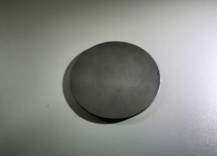
Germanium wafer
Germanium wafer , that it is widely used in the production of gold source in various electronic equipment, especially in solar cells and infrared applications, and the processes involved are more specific and complicated.
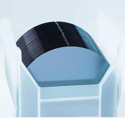
In the production process, we need to cut and grind the wafer. The wafer can be modified for different purposes, such as increasing its thickness and strength. We can reduce the surface roughness to reduce the generation of interface defects. Therefore, we can provide single-sided polishing and double-sided polishing processes.
Wafer substrate
Free Standing gan Wafer | Single Crystal Substrates
Si Doped Undoped Laser Device Gallium Nitride Wafer
300mm Gan Wafer | Gallium Nitride Wafer For Power Micro LED
8 Inch 12 Inch 6Inch gan Wafer
2 Inch 4 Inch GaN Wafer | Gallium Nitride Wafer
4inch 6inch GaN-ON-SiC EPI layer
Wafer substrate
What Is a Wafer Substrate?
Wafer substrate is used to support silicon wafers in the semiconductor manufacturing process.
Silicon wafer | Wafer substrate is the basic material of many electronic devices, which will affect the performance of the entire device. Therefore, when you choose the right integrated chip, it will determine the performance and process of your device.
N-type p-type and floating zone are the most common types of Guijinyuan. Although they are both crystals, their amorphous counterparts are also different.
Germanium wafer
Germanium wafer , that it is widely used in the production of gold source in various electronic equipment, especially in solar cells and infrared applications, and the processes involved are more specific and complicated.
In the production process, we need to cut and grind the wafer. The wafer can be modified for different purposes, such as increasing its thickness and strength. We can reduce the surface roughness to reduce the generation of interface defects. Therefore, we can provide single-sided polishing and double-sided polishing processes.