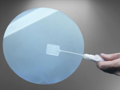
GaAs Wafers Supplier & Manufacturer in China
GaAs Wafers : Although silicon is undoubtedly the most popular semiconductor material at present, there are still many scenarios that are not suitable for application. However, Gallium Arsenide or GaAs wafers are rapidly becoming a very popular semiconductor raw material. Here, we will give you some advice on how to choose high-quality GaAs wafers sources.

2 Inch A - Axis Sapphire Wafer For EPI
5 Inch Sapphire Wafer R Plane Dia 125mm
8 Inch Sapphire Wafer Dia 200 mm
Gallium Arsenide (GaAs) Wafers
12 Inch Sapphire Wafers Dia 300mm
4 inch Sapphire Wafer C-Plane Single or Double Side Polish Al2O3 Single Crystal
6 inch Sapphire Wafer C-Plane Single or Double Side Polish Al2O3 Single Crystal
GaAs Substrate
GaIlium Arsenide (GaAs) wafers wide band gap has advantages that silicon lacks, including applications in high-frequency devices, high-power optoelectronics, and some semiconductors.
Who can provide high quality GaAs Wafers? XKH is undoubtedly a professional provider. In the field of Gaas wafers, please contact us now, for quotative to ensure timely delivery to you.
Our products include the following aspects :
N-Type Silicon Doped GaAs
P-Type Zinc (Zn) Doped
Chromium (Cr) Doped GaAs
N-Type Tellerium (Te) Doped GaAs Substrate
What size are GaAs wafers?
Gallium Arsenide Wafer
At present, our GaAs wafers have a relatively wide range of diameters, ranging from one inch to 11.8 inches.
We can provide some conventional models, ranging from 25.4 millimeters to 300 millimeters. We can also produce wafers of various thicknesses and directions and can provide polished and unpolished sides, as well as three dopants.
How thick is a GaAs wafer?
Gallium Arsenide (GaAs) Wafer, Size: 4”, Thickness: 300± 25 μm, Double Side Polished, We also offer single-sided polishing or no polishing processes.
It can be widely used in laser diodes, optical windows, high-frequency integrated circuits, infrared light-emitting diodes, and some barometers, and is also widely used in some monolithic microwave integrated circuits. Usually, we can see some high-temperature thermometers and air compressors, which have used GaAs wafers.
GaAs wafers are a compound synthesized by the combination of gallium and arsenic.This type of raw material mainly used in electronic products such as circuits, solar cells, and semiconductors has some advantages that silicon cannot match.
The migration rate of GaAs wafers elements can be artificially adjusted according to different levels of impurities.At the same time, GaAs wafers’ high saturation and electron mobility make it possible to use them in fast electronic switching applications and ultrahigh radio frequencies.
Technical Properties:
Quality | GaAs |
Materials | GaAs |
Size (inch) | 4” |
Thickness (μm) | 600± 25 |
Polished | Double Side |
Dopant | Undoped |
Orientation | (100) |
Resistivity | 1 E8 |
Mobility | 4500 |
EPD | ≤5000 |
| Original | China |
OF Length | 32,5±1 |
IF Length | 18±1 |
We also offer the following GaAs Wafers.
- Gallium Arsenide (GaAs) Wafer, Size: 4”, Thickness: 300± 25 μm, Double Side Polished, EPI-ready
- Gallium Arsenide (GaAs) Wafers, Size: 2”, Thickness: 350±25 μm, Double Side Polished, EPI-ready
Gallium Arsenide (GaAs) Wafers, Size: 4”, Thickness: 625±25 μm, Single Side Polished, EPI-ready
Gallium Arsenide (GaAs) Wafers, Size: 2”, Thickness: 400±25 μm, Double Side Polished, EPI-ready
GaAs Wafers, Double sided polishing with a thickness of 350±25 μm and two inches,dopant: Zinc (P Type)
We welcome you to inquire about our GaAs Wafer and other models of wafer. We will definitely provide the fastest delivery time and the best price.
Gallium arsenide wafer manufacturers : XKH
Silicon wafer is our another main products.