semiconductor substrate
semiconductor substrate : Look for high quality semiconductor substrate products and trusted professional semiconductor substrate manufacturers & supplier in China.Here is your right place, where you can get the professional info and substrate semiconductor prices you want.
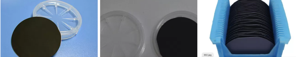
semiconductor substrate
Free Standing gan Wafer | Single Crystal Substrates
Si Doped Undoped Laser Device Gallium Nitride Wafer
300mm Gan Wafer | Gallium Nitride Wafer For Power Micro LED
8 Inch 12 Inch 6Inch gan Wafer
2 Inch 4 Inch GaN Wafer | Gallium Nitride Wafer
4inch 6inch GaN-ON-SiC EPI layer
semiconductor substrate
semiconductor substrate :Indium phosphide (InP) is a significant compound semiconductor material with high electronic limit drift speed, good radiation resistance, and high thermal conductivity. Suitable for the production of microwave devices and integrated circuits with high frequency, high speed, and high power. It is widely used in civil and military applications such as solid-state lighting, microwave communication, fiber-optic communication, solar cells, guidance/navigation, satellites, and other fields.
LEC (Liquid Encapsulated Czochralski) or VGF (Vertical Gradient Freeze) grown Indium Phosphide as epi-ready or mechanical grade with n type, p type, or semi-insulating in different orientations(111)or (100).
Indium phosphide (InP) is a binary semiconductor made up of the elements indium and phosphorus. It has a face-centered cubic (“zinc blende”) crystal structure, which is identical to that of GaAs and most III-V semiconductors. Indium phosphide can be prepared by the reaction of white phosphorus and indium iodide[clarification needed] at 400 °C.,[5] as well as by direct combination of the purified elements at high temperature and pressure, or by thermal decomposition of a mixture of a trialkyl indium Because of its superior electron velocity over the more common semiconductors silicon and gallium arsenide, InP is used in high-power and high-frequency electronics[citation needed].
Semiconductor Substrate Fundamentals
Industrial Semiconductor Substrate S Fe Zn Doped InP Indium Phosphide Single Crystal Wafer
Semiconductor substrates can be made from a variety of materials.
This article will go over a few key topics concerning semiconductor substrates, such as dislocations, polytype, and the process for forming continuous grooves.
It will also discuss the cost of semiconductor substrates.
Semiconductor substrate polytype
Polytype is a broad term for the structure of semiconductor materials.
It refers to a material’s crystalline structure.
It can be hexagonal or cubic in shape.
Because there may be more than one polytype of the material in semiconductor devices, it is critical to understand all of the possible structures.
Silicon carbide is a polytypic material with cubic and hexagonal crystalline structures.
Although the cubic form is not used in power devices, both polytypes have similar properties.
Both forms have properties similar to silicon, such as higher breakdown fields and a larger energy band-gap.
Here are some interesting facts about silicon’s two major polytypes.
Silicon carbide polytypes are created by stacking SiC molecules in a particular order.
The order in which these molecules are stacked is critical in the fabrication of semiconductor substrates.
It is critical to ensure that the growth conditions remain stable throughout the process.
Otherwise, spontaneous switching of polytypes may occur, affecting the material’s electric properties and acting as a defect nucleation site.
The polytype of SiC crystals grows in response to crystal growth conditions.
The first step in the fabrication of a semiconductor device is the formation of thin layers of semiconductor material known as epitaxial layers.
Using precise and well-understood techniques, epitaxial layers can be grown with high quality.
Slow growth rates, on the other hand, are required to produce high-quality epitaxial layers.