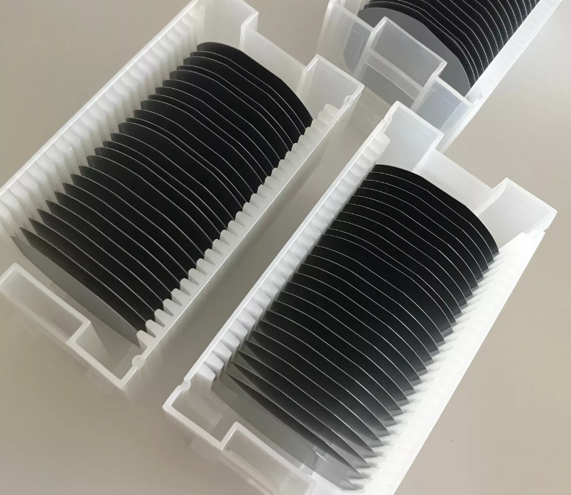
Silicon wafers
Silicon wafers: Silicon is a solid, reliable and high temperature resistant material. Due to its inherent stability, it is considered to be one of the best raw materials for building electronic circuits. It is widely used in computers, optical sensors and medical equipment. It is one of the most respected raw materials in the aerospace and automotive industries.
Silicon wafers:
We can provide high-quality and cost-effective silicon chips. Our inventory can meet your normal delivery needs.
We can also provide high-quality matt paper and silicon chips directly from 2 inches to 12 inches.Except dopped wafers, we can also supply un-dopped wafers.
At the same time, we can coating layer on silicon chips.such as SIO2 layer(Oxiden),SiN4 layer and so on.
Our optics and silicon windows are low cost and low density. In the optical plating of 1.2-76, it is very popular with users.
Silicon wafer (single side polished And double-sided polishing. ), P-type, 3 inch diameter and 0.5 mm thickness
At present, our monocrystalline silicon is excellent and cost-effective.
It is used in infrared optical materials and lenses for infrared optics. It is mainly used in high-tech fields such as thermal imaging systems and infrared mobile sensors.
And our materials have good thermal conductivity and thermal stability, and then relatively low, high expansion coefficient and relatively low density.