Silicon waffer
Silicon waffer :A silicon wafer is a material used in the production of semiconductors, which are present in a wide range of electrical products that improve our lives.
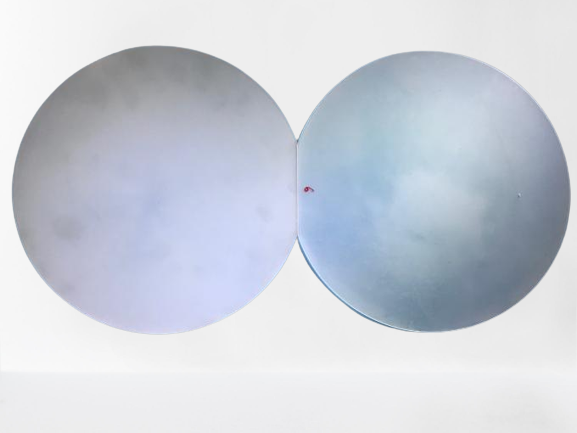
Few of us get the opportunity to interact with a real silicon wafer on a regular basis. This ultra-flat disk has been polished to a mirror-like surface and is as devoid of small surface flaws as possible, making it the flattest object in the world. It’s also ultra-clean, with virtually no microparticles or other contaminants. These properties are required for it to be employed as the substrate material for today’s cutting-edge semiconductors.
Silicon waffer
Free Standing gan Wafer | Single Crystal Substrates
Si Doped Undoped Laser Device Gallium Nitride Wafer
300mm Gan Wafer | Gallium Nitride Wafer For Power Micro LED
8 Inch 12 Inch 6Inch gan Wafer
2 Inch 4 Inch GaN Wafer | Gallium Nitride Wafer
4inch 6inch GaN-ON-SiC EPI layer
Silicon waffer
Silicon waffer
An easy approach to give a metal part’s surface a nicer finish is to use a silicon waffer for surface grinding. Additionally, it is a reliable approach to accomplish it without damaging the part’s edge.
surfaces are ground :Silicon waffer
Numerous studies have documented grinding techniques causing harm to silicon wafers. Subsurface cracks’ prevalence and distribution, however, are not completely understood.
Three process variables have been examined statistically to see how they affect the development and distribution of subsurface cracks. A three-factor, two-level, full factorial design was used to create this study. This technique can be used to determine how three process variables interact with one another.
Due to surface tension, molten silicon is redistributed in the flow throughout the grinding process. In the course of laser grinding, this phenomena has been seen.
Cell for anodization : Silicon waffer
A crucial step in the creation of devices is typical semiconductor anodization. Anodization applications, however, have not yet become widely used. The anodized films’ quality is impacted by a number of variables. One of the key elements is the electrolyte used in the anodizing process.
There are two primary stages to the anodization procedure required to create a high-quality silicon wafer. The silicon wafer is first rapidly anodized. It is then chilled in a bath of cold water. This guarantees that there won’t be any localized heating of the chemical.
By adjusting the current density during the anodization process, the porous silicon layer’s porosity can be made more porous. There aren’t any established guidelines for the current density that will produce a dense layer of silicon, though. The type of electrolyte used and the potential provided during the anodizing process affect the interpore distances.
The length of the anodizing procedure can also affect how thick the porous silicon layer is. Additionally, by lowering the concentration of the anodization electrolyte, the pore size can be enhanced.
One to 50 mm can be used as the range for the top porous silicon layer’s thickness. The top porous silicon layer should be between one and 50 mm thick at its ideal thickness. The layer essentially stays the same during subsequent etching.
Anodizing a silicon specimen at a rate of 25.8 mA/cm2 for 20 minutes created the bottom silicon porous layer. A step of high-temperature annealing in argon followed this. Si-H bonds are broken and the surface is smoothed during the annealing process. The pores in the top porous silicon layer are likewise sealed off during this annealing process.
Doping :Silicon waffer
There are numerous techniques for doping semiconductors. For illustration, boron has been doped into p-type silicon wafers. Because electrons move through the circuit in the same direction, resulting in a minimal net current flow, this material is useful for solar cells. Additionally, back-side lighting for minority carriers is not necessary for p-type silicon wafers.
Applying a doping solution to silicon particles is how silicon particles are doped using thermal diffusion. To reach the required doping level, the temperature of the doping solution is adjusted. Doping concentrations are typically between 10 and 45 percent of the available boron in the solution. To make the procedure simpler, the approach can be used in conjunction with continuous melt replenishment.
A low boiling solvent, such as ethyl alcohol, makes up the boron doping solution. The solvent may also be diluted with antimony or arsenic.
A dispenser dispenses the doping solution. The silicon feedstock pellets are then injected with the boron doping solution. Next, the pellets are combined with drying in one step. If the wet stock has no lingering odor, it has been totally dried.