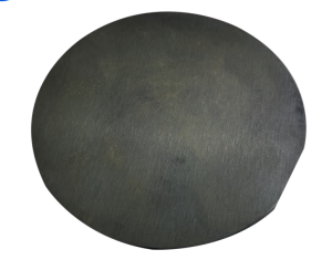
GaN Wafer
20 years of deep cultivation in the sapphire industry just for continuous production of high-quality gan on si wafer.
Your Reliable GaN Wafer Supplier in China
Gan wafer | Your Leading supplier & manufacturer in China,To supply your gan epi wafer,gan on si wafer and gan on silicon wafer with good price and many kinds of size. According to the real gan wafer market situation,We are your trusted gan wafer suppliers .
GaN Wafer : When our GaN wafer is applied to laser, it has Higher Yields and Lower threshold voltage with Higher power.In LED field, it has good Better efficiency. In Transistors, it has Lower leakage current and Higher power.
Gan wafer size is widely,include 8 inch, 6 inch,12 inch, 2 inch, 4 inch ,5 inch etc.
We must emphasize that our gallium nitride substrate is a high quality single crystal substrate, which is manufactured by a unique process and method and Gan wafer processing technology. Its main characteristics are its high cleanliness, obvious surface quality and excellent uniformity. In the production of LED, gallium nitride substrate is widely used, especially purple, blue and green.
In addition, great progress has been made in the application of power and high–requency electronic equipment in the future. To achieve lower defects and higher productivity, we have been developing new technical means to produce high quality GaN substrates.
Choosing Your GaN Wafer from Manufacturer
Si Doped Undoped Laser Device Gallium Nitride Wafer
300mm Gan Wafer | Gallium Nitride Wafer For Power Micro LED
8 Inch 12 Inch 6Inch gan Wafer
2 Inch 4 Inch GaN Wafer | Gallium Nitride Wafer
4inch 6inch GaN-ON-SiC EPI layer
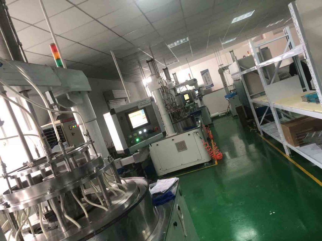
Semiconductor Wafer Manufacturing with GaN
Over 15 years experience
One-stop Sapphire Wafer supplier & manufacturer
Full Range Varieties of Sapphire Wafer
Good experience cooperating with world-renowned companies
Sapphire Wafer includes 2 inch, 4 inch, 5 inch,6 inch,8 inch, 12 inch etc
Your Leading Gallium Nitride Sapphire Wafers Manufacturer in China
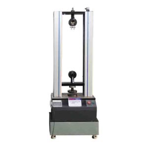
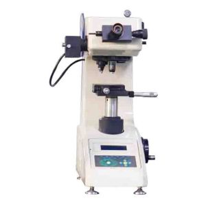
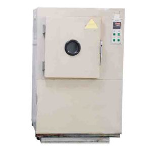
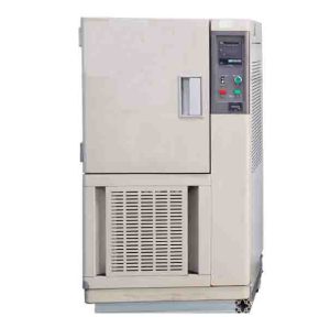
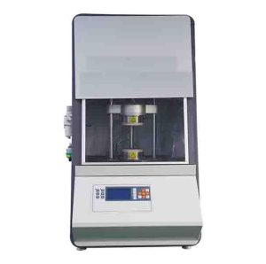
XKH will use specific high-end and advanced testing equipment to test our sapphire related products to ensure that every product you have is efficient and stable.
Gallium Nitride (GaN) on Silicon (Si) Epitaxy Wafer
Do You Experience The Issues When Buying From China
- Hard To Find A Professional aftermarket Sapphire Substrate Supplier & Manufacturer in China,But Foreign Trade Companies Without Guarantee.
- Long Lead Times Of Sapphire Substrate From China,Delivery Time Non – Guaranteed.
- Uneven Quality of Chinese Sapphire Wafer,The Sellers Can not Guarantee The Life Time of Sapphire Wafer.
- Few China Suppliers Can Provide Solutions When You Face Quality Problems
- Rarely Possible To Cooperate with China Factories That Hace Full Service With Strong R & D Team,Manufacturing,Selling, After-Sale Service, And Technical Support.
XKH Will Be Your Trust Gallium nitride (Gan) wafers Supplier
With 15 years of market experience, the Sapphire Wafer of XKH has been recognized by customers in many countries. We are very grateful to users for their support and trust over the years.

At the beginning of GaN nitride procurement, we compared many suppliers and manufacturers in China, and finally, we chose the New Science and Technology Association because we found that their price and quality have dual advantages.
John Doe

If you choose XKH’s gallium nitride wafer, you will get concrete and substantial help in your marketing and production, because their technical team is very strong, which can help you save a lot of time and energy. Please choose a cartoonist from the New Science and Technology Association. The gold dollar is your right decision.
Jessica Smith

In the end, we were lucky to choose Xinkehui as the manufacturer and supplier of our sapphire wafers. Their sapphire wafers are excellent, and our customers are very satisfied with this, especially in terms of price and quality stability. You can purchase from Xinkehui with complete confidence.
Steve Rogers
GaN Wafer - Gallium Nitride - FAQ
As a leading gan wafer suppliers,we have greatly reduced the current energy consumption, and are considered to be the booster of breakthrough progress in the field of high–ower electronics and solid–tate lighting. Our quality has a very high electron streamer concentration and intensity in the production of potassium nitride.Its lattice and its platform,Its dislocation density is at least two orders of magnitude lower than that of substrates produced by other technologies.
Gallium Nitride Wafer
GaN (gallium nitride) substrates and wafers with high quality (low dislocation density) and best prices on the market.
The output and power of high gloss devices, RF devices and power devices come from the high crystallinity of GaN wafers.
GaN wafers can be used as projector light sources and one side of electric vehicles. At the same time, To achieve unprecedented super brightness, laser diodes and high efficiency devices are a major function of GaN wafers.
We are pleased to see that the potassium nitride GaN wafers crystallized from the liquid equilibrium system has a very high cleanliness, which can hardly be found few dislocations.
In addition to improving reliability, high cleanliness also helps to improve the output and efficiency of optical devices, radio frequency devices and power devices made of these wafers.
GaN Wafer (GaN substrate)
Realizes high crystallinity
crystallized from a liquid-phase equilibrium system exhibit remarkably high crystallinity, with.
In addition to improving reliability, high crystallinity helps increase the output and efficiency of optical devices, RF devices, and power devices manufactured using these wafers.
We have developed a large–cale production structure of two inch diameter GaN wafers for laser diodes and other light source equipment, mainly used in RF devices and power devices. Our goal is to strive to increase the diameter and reduce the dislocation density, strive for large–cale production, which can help more users.
We have several types of Gallium Nitride Wafer , including M-type, P-type and semi insulating insulating gallium nitride .
His template is a gallium nitride epitaxial wafer with defect density. Our variety is not only complete, but also includes gallium nitride substrate substrate, gallium nitride on SIC/Silicon and sapphire,
LED epitaxial wafer with low defect density, and gallium nitride hemt epitaxial wafer .
High Quality GaN Substrates & Wafers
150mm DesiGaN Power/RF HEMT Series
For gallium nitride wafers with a diameter of 100 mm to 200 mm, we have enough stock for you to choose from, and we most accept your minimum order quantity.
For the application of high-voltage resistors and RF circuits, we have a better RF HEMT Series of Gallium Nitride on Silicon (GaN-on-Si) is an AlGaN/GaN hetero-epitaxial layer structure grown on a Silicon(111) substrate to supply for you.
Typical Application
*Power HEMT
*RF HEMT
*GaN Diode
Advantages of Gallium Nitride Wafer.
Higher operating temperature,
high breakdown voltage,
lower on resistance,
higher switching frequency,
higher operating frequency and high uniformity.
High Crystallinity of GaN Wafers Helps Increase the Output
We have provided high quality GaN epitaxial wafers, and we have 15 years of experience.
In the process of continuously improving the process, we are constantly improving the quality of our desalinated grade Gan wafers.
Our goal is to produce gallium nitride substrate with controllable surface orientation and very flat surface, so that it is undamaged and has controllable atomic ladder surface. Fortunately, our epitaxial growth technology is very outstanding at present.
We have been making unremitting efforts to produce GaN substrates with high linearity and higher productivity.
Applications
- Laser : violet LED, blue LED, and green LED
- Power electronic devices, High frequency electronic devices
8-inch GaN-on-Si Wafers Manufacturing Technology
By simultaneously processing more devices on each semi-gallium wafer, the overall cost can be decreased.
Consequently, 8-inch wafers might obtain 80% more time per wafer than 6-inch wafers, which will surely increase production prices. Therefore, potassium nitride device technology can make production more cost-effective.
Gallium Nitride Wafer | GaN Substrate
RF GaN wafers for GaN-on-Si applications
On the gauge, gallium nitride has a wide range of gap. Such as integrated transistor circuits and diodes, the electronic circuits that make this substance important to electricity.
The gauge band gap of GaN semiconductor is three times that of silicon, and thus broadband dilutor offers a broader range of voltage and temperature applications.
Potassium nitride is an outstanding semiconducting material. It is unique due to its optimal selection of low-resistance RF and high-frequency components.
Due to its low price, it is a desirable raw material for a variety of electronic applications. It is less expensive than tortoise. It is a market leader in numerous application domains due to its low pricing.
Potassium nitride with its low-voltage characteristics is a perfect semiconductor for automotive applications. Its low-voltage qualities also make it the best material for high-power transistors and power converters. And it is not easily heated.
What is gallium nitride used for ?
Gallium nitride is mainly used in semiconductors, components, video components, lasers and photonics.
In the near future, you will also see our application of gallium nitride in sensors, which is under our practice and exploration. Of course, the blue light emitted by a single nail is mostly used for reading blue optical discs, which is a relatively common application at present.
Gallium nitride wafer price
At present, the price of potassium nitride in the market is uneven. The final price of gallium nitride will be sold in the market in a very different way depending on the different raw materials, processes and suppliers’ quality.
Therefore, we suggest that you first choose a more reliable supplier of gallium nitride, and then discuss the price.
However, the quality is always the first at any time. The price of gallium nitride varies greatly according to the quantity you purchase. Therefore, we will broadcast our lowest price for your reference according to the specific application and quantity.
Do you use these keywords to find us? For example gan wafer,gan wafer size,gan epi wafer,gan on silicon wafer,gan wafer market,gan wafer price,gan wafer suppliers,gan on si wafer,gan epi wafer capacity,gan epitaxial wafer,gan hemt wafer,gan on sapphire wafer,gan on si wafer price,gan on sic wafer, and gan wafer,gan wafer cost,gan wafer manufacturer,gan wafer thickness,hemt gan wafer,led gan wafer,typical cost of a 6 gan wafer etc, Anyway, I hope you can finally find us, and we can provide you with professional technical support and price support.