Gallium Nitride Wafer
Gallium Nitride Wafer
Free Standing gan Wafer | Single Crystal Substrates
Si Doped Undoped Laser Device Gallium Nitride Wafer
300mm Gan Wafer | Gallium Nitride Wafer For Power Micro LED
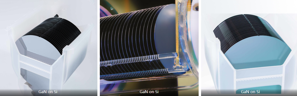
8 Inch 12 Inch 6Inch gan Wafer
2 Inch 4 Inch GaN Wafer | Gallium Nitride Wafer
4inch 6inch GaN-ON-SiC EPI layer
Gallium Nitride Wafer
Gallium Nitride Wafer Applications
Gallium Nitride Devices (Discrete & IC) and GaN Wafer are classified into two markets: device type and application. The market is divided into four regions: North America, Europe, the Middle East, and South America.
Gallium nitride’s high-frequency properties make it an excellent candidate for high-frequency semiconductor applications. The material is also non-toxic and can be used in electrodes. Gallium nitride is a less expensive and more flexible alternative to silicon for power-efficient systems.
Gallium nitride’s bandgap on silicon makes it an excellent choice for high-frequency devices. It is more stable at higher temperatures than silicon due to its wide bandgap. This is a significant benefit in high-frequency and high-power applications. It is also more secure than silicon, making it an appealing option for sensitive electronic equipment.
Gallium Nitride semiconductors have emerged as a viable option for high-frequency power solutions in recent years. They are ideal for high-voltage, power-efficient transistors and power converters. GaN wafers are an excellent choice for such applications due to their high breakdown voltage and low power loss. Furthermore, they are less susceptible to heat than silicon, making them a more versatile option.
Gallium nitride semiconductors are increasingly being used in automotive and hybrid power conversion. This new material is also being used in solar power installations and motor drive power conversion systems. Its wide bandgap enables faster switching rates than silicon, the traditional material for these applications.
In a number of applications, gallium nitride semiconductors have already surpassed silicon . These devices are faster and more efficient than silicon, and they can operate at higher temperatures and voltages. They are also more robust and resistant to high temperatures.
Power amplifiers are yet another application for gallium nitride semiconductors. These power amplifiers are applicable to wireless communication systems. This will improve the efficiency and cost-effectiveness of these communication networks.