Your Reliable Sapphire Wafer Supplier
Xinkehui is a well-known industrial sapphire wafer manufacturer and supplier in China. We can provide you with different kinds of professional silicone wafers,Sic Wafer, including Gallium Nitride Wafer,Sapphire Wafer,SiC Substrate , Indium Phosphide Wafer,Sapphire Optical Windows,Sapphire Parts, Sapphire Cover Glass,GaAs Wafer,Synthetic,Sapphire Rod,Synthetic Ruby,IC Silicon Wafer,Fused Quartz Plate,Ceramic Substrate and Synthetic Sapphire Block.
After more than 20 years of experience, new customers can also provide you with complete sapphire related products, and support your high-quality demand and low price market competitiveness. We guarantee that more of our products will arrive in your hands as soon as possible. Please do not hesitate to contact us.
Sapphire wafer| Sapphire substrate| Window| Ingot
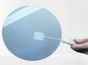
2 Inch A - Axis Sapphire Wafer For EPI
Sapphire optical chips, 2inch sapphire substrates for led & Epi
5 Inch Sapphire Wafer R Plane Dia 125mm
5 Inch Sapphire Substrate | Al2O3 Material | 9.0 High Hardness
8 Inch Sapphire Wafer Dia 200 mm
8inch C plane sapphire wafer, Al2O3 crystal optical lens
12 Inch Sapphire Wafers Dia 300mm
1.0mm Double Side Polished Sapphire Crystal Glass Wafers
4 inch Sapphire Wafer C-Plane Single or Double Side Polish Al2O3 Single Crystal
85% Light Transmissivity for Led
6 inch Sapphire Wafer C-Plane Single or Double Side Polish Al2O3 Single Crystal
Al2O3 Crystal Optical Lens For LED Epi
China Sapphire Wafer
Over 15 years experience
One-stop Sapphire Wafer supplier & manufacturer
Full Range Varieties of Sapphire Wafer
Good experience cooperating with world-renowned companies
Sapphire Wafer includes 2 inch, 4 inch, 5 inch,6 inch,8 inch, 12 inch etc
Your Professional Sapphire Wafer Manufacturer in China
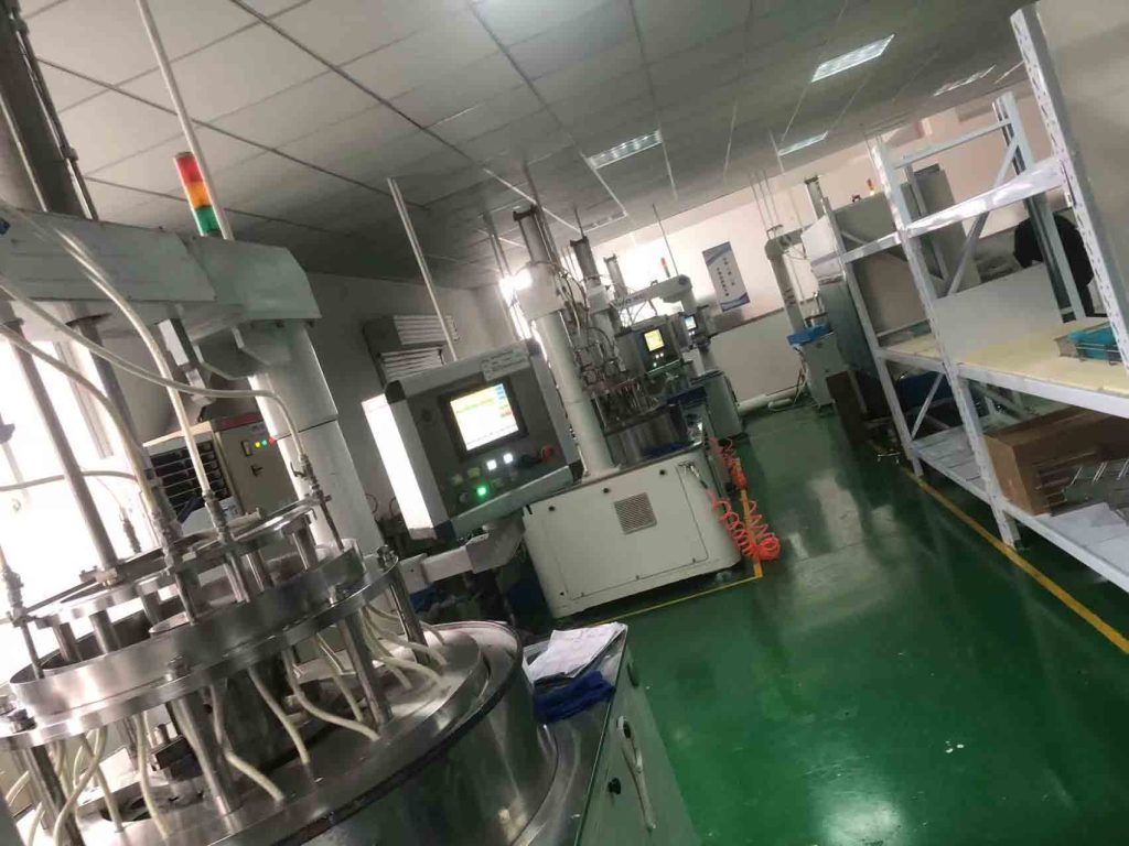
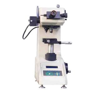
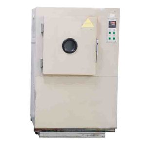
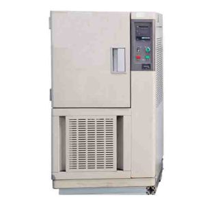
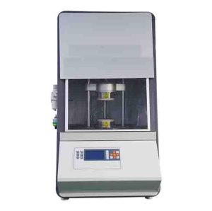
XKH will use specific high-end and advanced testing equipment to test our sapphire related products to ensure that every product you have is efficient and stable.
上一页
下一页
Sapphire Substrate
Do You Experience The Issues When Buying From China
- Hard To Find A Professional aftermarket Sapphire Substrate Supplier & Manufacturer in China,But Foreign Trade Companies Without Guarantee.
- Long Lead Times Of Sapphire Substrate From China,Delivery Time Non – Guaranteed.
- Uneven Quality of Chinese Sapphire Wafer,The Sellers Can not Guarantee The Life Time of Sapphire Wafer.
- Few China Suppliers Can Provide Solutions When You Face Quality Problems
- Rarely Possible To Cooperate with China Factories That Hace Full Service With Strong R & D Team,Manufacturing,Selling, After-Sale Service, And Technical Support.
XKH Will Be Your Trust Sapphire Wafer Supplier
With 15 years of market experience, the Sapphire Wafer of XKH has been recognized by customers in many countries. We are very grateful to users for their support and trust over the years.

Your sapphire wafer products are very good, transparency is very nice , and have a very wide range of applications, especially the price competition. In our market, we have your support, which makes us even more powerful.
John Doe
Vancouver

We have been purchasing sapphire wafers from XKH for 6 years. Their quality has been very stable and delivery has been very timely, especially in terms of technical support.
Their engineer team is very strong. We are very grateful for your help.
Jessica Smith
Toronto

In the end, we were lucky to choose Xinkehui as the manufacturer and supplier of our sapphire wafers.
Their sapphire wafers are excellent, and our customers are very satisfied with this, especially in terms of price and quality stability. You can purchase from Xinkehui with complete confidence.
Steve Rogers
Montreal
Sapphire Substrate Wafers - FAQ
As a professional sapphire (Al2O3) wafers supplier and provider, we are trusted by most customers all over the world because of our stable quality. Our Sapphire Wafer is also called Al2O3. Its product range includes 1 inch,2inch,3inch,4 inch,5inch,6 inches, which have a large amount of inventory to ensure your timely product needs. We can also customize the special saphire substrates according to your needs.
Sapphire Wafers
Sapphire Window Sale
If you happen to be looking for Sapphire wafer substrate manufacturers for LED power semiconductor, watch glass and sapphire wafers for other sapphire substrates, it is a right decision for you to contact us, because we are constantly researching and exploring the manufacture of sapphire wafers, and I believe we can help you.
What are Some Sapphire Applications?
In fact, the application range of sapphire wafer is extremely wide. It can not only be applied to the electronic field, but also the planar sapphire substrate has been used in the photoelectric field for decades, such as microscopes, flat panel displays, etc.
That is to say, any surface application of sapphire wafer can be involved. By placing an electrode in the substrate, a thin metal oxide layer can be created, Absorb all ultraviolet rays that shine on the display or microscope. As a result, the human eye cannot see them at all.
Now science is promoting these planes, which are basically used in the photovoltaic field, such as creating solar cells and solar concentrators.
So at present, sapphire is not only used in some scientific fields, but also used in some engagement rings as a common application.
In terms of scientific application, it mainly depends on planar sapphire, which can be used in photoelectric effect measurement, fluorescence and chemical analysis. It is mainly because sapphire has a very obvious feature that it allows most colors to pass through, Why is that?
Sapphire can be an engagement ring. The reason why it can be used is that it can be transparent or opaque.
Although it is impossible to make various colors on sapphires for engagement rings at present, we can see from the color perspective that sapphires from yellow green to blue white are also commonly used as rubies and emeralds. Of course, it is the most common application designed for watches and cuffs.
Sapphire Window Orientations
At present, there are two main ways to develop sapphires for optical applications. One is called m axis, and the other is called 2 Axis. Android is relatively complex.
It involves relatively accurate crystal arrangement, which is composed of ordinary elements. There is a flat chisel in the center to align with a specific rotation axis. It is usually called square angle alignment, also called wave plate, which is the principle of generating a high quality diagram line from a plane circle.
The two sapphires are basically based on the same optical measurement.That is, birefringence.
This refraction method is used to measure the crystal imbalance when light waves hit the light source. The best measurement of birefringence is when the crystal is completely spherical.
Because crystals close to the spherical shape have higher birefringence than those slightly irregular crystals, high birefringence can improve the clarity of the image generated by sapphire, and improving its brightness is conducive to better color performance.
The key reason for the influence of sapphire crystal orientation is the stimulation of sapphire crystal and whether the top surface is flat?When a photographer chooses a fast lens, the faster the lens is, the clearer the image will be. This is why they must consider sapphire and its direction.
The S angle is an important attribute of sapphire. It indicates the direction of the crystal on a plane with observation windows overlapping.
In short, when the observation window coincides with the symmetry plane of the sapphire, the birefringence is balanced. When the window and the gemini are not coincident, the sapphire will show positive birefringence.
We provide services for high-quality semiconductor equipment and epitaxial growth.
It is characterized by high-quality cleaning, as well as Dick’s ability to absorb metal pollution.
Substrate drilling, slotting, cutting and back polishing, etc.
The cleanliness and shape of the substrate we provide are available for you to choose from.
Very high flatness.
Our specifications are very much. They can be selected from two inches to eight inches, or substrates with a diameter of 300 mm are available. If you need any kind of sapphire, you can contact us.
The unique growth method we adopt is our body, that is, the film growth method defined by the edge.
By growing single crystal sapphire into sheets, we can make the sapphire chips meet the requirements of quality cost and delivery without additional processing.
In addition to listening to the general standards and substrates used for LED, we also provide higher quality gold and chips, which are used for high quality and clarity, The resulting low particle and low metal pollution is a very good progress.
Our precision manufacturing technology controls the flatness and minimizes the possible warpage problem in epitaxial growth. High quality essence is the best choice for new process product development.
Therefore, if you are an LED user or need to use our sapphire gold source for RF devices of electronic products, please contact us.
Sapphire Wafer
CAS #:
1344-28-1
Linear Formula:
Al2O3
The high qurity single crystals, sapphires and wafers produced by us for optoelectronic applications, whose standard wafer diameters range from 1 inch to 11.8 inches, that is, 25.4 mm to 300 mm, can even produce polished or non polished surfaces of various thicknesses, and can include the current gold source sapphire wafers, which have been widely used in 4G, technology, food, agriculture, pharmacy and optical grade.
We can also produce material specifications according to customer requirements, provide standard customized packaging and make further research in technology.
Sapphire
Sapphire Wafers
We are a major supplier and provider of sapphire substrates, which are mainly used in optoelectronic applications and high-brightness LED markets.
Make every effort to make one or both sides of the substrates extremely smooth and undamaged. The growth and orientation of materials, as well as the production and polishing of substrates, are our daily operations. We have a variety of business directions and diameters for customers to choose from.
- A-Plane sapphire substrates – This material is mainly used for electronic applications where high insulation properties and uniform dielectric constant are required.
- C-Plane substrates – Prefer to be used for cutting bright blue and green LED and laser diode.
- R-Plane substrates – It is the silicon in microelectronic IC applications and the first choice for heteroepitaxy.
3 inch Sapphire Wafer C-Plane Single or Double Side Polish Al2O3 Single Crystal
Up to now, sapphire is the strongest and most resistant to thermal shock and chemical corrosion, and it is widely used as an ideal material for electronic substrates.
The sapphire substrate has many planes, including c plane, a plane, and b plane. At present, the black sapphire lens is the most widely used sapphire substrate, such as potassium nitride or gam, and the bright blue and green LEDs of laser diodes all use this product material.
It is also applied to ordinary optical devices, when the infrared or ultraviolet range is required. Sapphire substrate is a suitable substitute for glass substrate.
Gallium nitride epitaxial layer grown on A idea sapphire can be used for mixed microelectronic and optoelectronic applications. Sapphire substrates are widely used in various industries according to their different plane directions and configurations.
A plaine is mainly used in integrated circuit and photovoltaic fields at the regulatory level.
C plane sapphire lens is the most widely used sapphire substrate at present. The compounds it is used to grow include gallium nitride or bright blue LED lamps, and it is also used in infrared detectors.
Sapphire is one of the most important substrate materials. The characteristics mentioned above determine the characteristics and application range of sapphire substrate.
In terms of manufacturing process, the first requirement of sapphire lenses is plane orientation.
Check the structural matching between the substrate and the epitaxial film. You need to precisely position the sapphire crystal bar on the slicer and cut it into thin slices, then remove some debris to make it smooth, and make its edges smooth. After being trimmed, you need to do this.
The roughness is removed by polishing. Finally, the dust particles on the surface are cleaned without pollutants. Finally, the test is carried out to check the quality of the substrate with a high–recision instrument to determine whether the sapphire can meet the customer’s needs.
Sapphire has excellent electrical insulation, transparency, thermal conductivity and high rigidity. It is an ideal substrate material for microelectronic circuits, ultrahigh speed integrated circuits and LED clocks. Its a–ide and a–ide are used to produce non solar semi polar planar epitaxial layers, improve its luminous ability, stable dielectric constant and DJ electrical loss, making it very useful in mixed microelectronic products.
What is sapphire substrate?
Sapphire is a unique combination of chemical and physical properties. It has strong resistance to the erosion of high temperature sand and water. Its thermal conductivity is excellent even at low temperatures.
It is substrate made of sapphire.
Purchasing Sapphire Substrate
Sapphire substrate provides different prices in different suppliers, and there are different ways to sell this raw material on the network. Of course, we think that price and quality are two key points that you must consider.
At present, it is basically made of sapphire, which is a material with unique chemical optical and physical properties. Basically, if you want to buy it, you can contact us.
It is widely used in infrared ray, optoelectronics and electronics as well as silicon integrated circuits on sapphire to produce unique mechanical properties of substrates.
There are many sizes of sapphire substrates of different sizes for you to choose. You can choose the correct size for your body according to your specific requirements.
Sometimes you may need several sizes to meet your needs. No matter what the situation is, the most important thing is that you can find a supplier with professional capabilities like us that can not only meet your needs of various sizes, Providing can also provide a strict control over quality, which is for you. The sapphire substrate is the most powerful guarantee.
In washing machines, digital cameras, smart phones, watch LED bulbs and refrigerators, semiconductors or semiconductors are used. Of course, they are also used in integrated circuits, so there will be more development in the field of sapphire substrates, in the future industrial development.
Sapphire Wafer Dia 25.4mm, Double Sided Polished
As a leading supplier of sapphire wafers, our company has introduced 6 inch, 8 inch and 10 inch sapphire wafers to the market.
Most of our products are grown on sapphire wafers. We have always been the leader in the 6 inch and 8 inch wafer markets, and the key parameters of LED depend on the surface quality of the sapphire substrate.
The high quality of our sapphire wafers has helped our customers play a positive role in producing LED brightness and reducing wavelength distribution.
Our production and research and development of polished sapphire wafers are mainly to help our customers achieve unique advantages in the LED market.
The new technology we developed improves and enhances our experience by reducing the internal stress of growing crystals, enhancing the geometric shape of wafers, and creating unique cleaning technologies to meet customers’ current needs and market trends, which is why we were able to exit, conform to LED and Ultravision, and help our customers increase their output.
Sapphire itself is a material combining physical, chemical and optical properties. It has extremely strong resistance to high temperature, thermal shock, water and sand for instructions and scratches. It is an excellent window material, suitable for many infrared applications ranging from 3 microns to 5microns.
C Plane and sapphire substrates are widely used to grow III-V and II-VI compounds, such as stores for blue LEDs and laser diodes, and sapphire substrates, Heteroepitaxy of silicon for microelectronic IC applications.
Its feature is that the 2 Inch sapphire wafers can be reduced to 250um,4 inches can be reduced to 300um, and 6 inches can be reduced to 300um.
sapphire wafers have excellent strength, Thermal Stability, and Chemical Stability.
Sapphire Wafers for Electronic Devices
Sapphire substrate and sapphire gold source have excellent material properties and can be used for mass production. In order to meet the increasing needs of customers, we will continue to increase the size of the wafer and strengthen the demand for particle suppression.
Materials: Single-Crystal Sapphire | Silicon on Sapphire Substrates
Sapphire Substrates for LEDs
We have been persistently researching and developing high quality sapphire wafers and optical windows for many years, and have been the leader among many export enterprises. With years of experience, we have provided standard and customized sapphire wafers from one inch to eight inches, which can be used in any direction and thickness of extension, and sapphire windows of any specification for sapphire optics.
We can also provide patterned sapphire substrates and sapphire crystal bars for customers to meet their needs.
We have strict production procedures. From raw material procurement to the transportation of high optical sapphire products, we carry out full inspection before leaving the factory.
A piece of gold in Meimei has undergone strict inspection before shipment. All our employees will do their best to ensure that the quality of the sapphire lenses you have is perfect, and we are also very punctual in terms of delivery.
As a well known sapphire substrate manufacturer for many years, we have provided optical sapphire products and technical support to hundreds of customers around the world, including some world-leading epitaxial companies, sapphire optical device manufacturers, university laboratories and scientific research institutions.
SILICON ON SAPPHIRE
The silicon on sapphire is an epitaxial process used for manufacturing metal oxide semiconductor integrated circuits.
It includes thin layer (typically thinner than 0.6 µm) of silicon grown on sapphire wafers.The high-purity synthetic sapphire crystal they used is the main material.
GAN ON SAPPHIRE
In the production of blue or green LEDs, one of the main materials is GaN nitride, because they combine the electrical part with the optical part of the LED to improve the efficiency of LED products. The growth on the sapphire substrate is that the LED has a thorough insulation performance, but has current transmission.
LED SUBSTRATES
We have mentioned many times that sapphire is mainly used for LED. The sapphire substrate has the characteristics of high temperature resistance, high strength, good electrical insulation, energy and low dielectric loss. It is the best choice for LED applications.
The sapphire substrate helps prevent stray current caused by radiation from spreading to nearby circuit components in LED lighting. Its crystal structure also enables LED lamps to have a wider beam angle.
We provide standard and customized sapphire wafers to meet your needs for optoelectronic applications. Due to the small format of sapphire gold, stable chemical and physical properties, sapphire wafer superconductors and commonly used devices for magnetic epitaxial hair, they are widely used in the market and optical industry on potassium nitride and thin film epitaxial growth sapphire.
As a professional manufacturer of sapphire wafers, the standardized and customized sapphire wafers we provide can be used for sapphire windows of any specification in optics, and can also be used in any direction of epitaxy.
We can also provide patterned sapphire substrates and sapphires. It is destined that we are the experts in the manufacture of sapphire optical devices.
SAPPHIRE WAFERS / SAPPHIRE SUBSTRATES
Sapphire wafers are commonly used as substrates for superconductors and magnetic epitaxial films because of their few lattice adaptations and stable chemical and physical properties.
It is widely used in the silicon LED market and optical suppliers of potassium nitride and thin film epitaxial growth sapphire.Our sapphire substrate has excellent surface finish, which is why it is respected and applied to LED. If you are looking for a reliable sapphire wafer supplier, please contact us immediately.
We can provide all high-quality surfaces of sapphire wafers. (C-plane, A-plane, R-plane, M-plane, N-plane, V-plane, 10-14 etc.) If you have no special needs, we can also customize sapphire wafers for you.
The surface roughness of our products is very low, and there are complete direction choices.
We not only provide round sapphire lenses, but also square and rectangular sapphire substrate wafers. We provide a wide range of sizes : 5mm x 5mm, 10mm x 10mm, 10mm x 15mm, 15mm x 20mm, etc.
Features of single crystal sapphire
- Sapphire has the characteristics of transparency, high rigidity, good thermal conductivity, electrical insulation, etc. For these reasons, it can be used as a substrate material for integrated circuits, such as electronic circuits, LED, and even ultrahigh speed integrated circuits.
- Sapphire substrates are often used in harsh environments, such as, uh, precision manufacturing of gas detection sensors and detector windows such as bearings, and scanners of commodity bar codes.
- All these are due to the high rigidity, high strength, high temperature, stability, wear resistance, corrosion resistance and other characteristics of sapphire, which make it widely used in these difficult fields.
- Sapphire is also widely used as electronic tube dielectric material, ultrasonic conductive element and other optical elements. Because of its good optical transmittance, sapphire is also widely used in some infrared military devices, high–ntensity lasers for space vehicles and optical communications.
Excellent SAPPHIRE WAFERS
- As a well-known sapphire wafer manufacturer in China, we have been committed to providing high-quality sapphire substrates for your business.
- Most of our specifications are in stock, which can ensure timely delivery for you.
- The standard export packaging ensures the safety during transportation and saves your costs.
- For all batches of sapphire wafer, we have batches to track, with serial numbers.
- The packaging is very flexible. There are 25 packages in a box as well as a single package.
- Clean the clean room with ultrapure water of high quality.
- It has excellent surface quality in all directions, including A plane , B plane , M plane , N plane and V plane .
- The excellent polishing technology ensures the performance of the sapphire substrate and the cost control is particularly excellent.
- 99% high purity single crystal Al2O3 material.
LOOK AT WHERE SAPPHIRE WAFER APPLIED
So far, our polished sapphire lenses and unpolished sapphire lenses are widely used in the semiconductor microelectronics industry and LED industry.
The products are widely used in hybrid microelectronics.
Generally, this industry has high requirements for substrates, and the characteristics of sapphire substrates are stable dielectric constant and DJ electrical loss, making them the most commonly used raw materials in the microelectronics industry.
Generally, a-side sapphire wafers are required.
Semiconductor LED industry,epitaxial GaN substrate)
In this field, we suggest to use sapphire with c plane, while R plane and M plane are mainly used for growth non polar single, polar plane and epitaxial layer are grown to improve luminous efficiency.
The application of microelectronic integrated circuits, especially those with high speed and good luck.
Generally, it is a silicon heteroepitaxial deposition on R-plane sapphire.
sapphire wafer processing
First we need a crystal boule . High quality sapphire single crystal sapphire is produced through crystal growth, processed in the shop, drilled out the crystal rod, ground the crystal rod, and then inspected for quality. Then we get the sapphire ingot
Then place the crystal bar on the sawtooth machine, and cut it into slices for rolling. This grinding process can remove scratches and improve its flatness and smoothness, and trim the edge of the gold source into an arc to improve the mechanical strength and avoid stress concentration.
Then we need to polish to improve the smoothness. Then we need to clean to remove the dirt on the surface. Then we need to carry out quality inspection. We need to check Qingyuan with high-precision instruments to meet the specific requirements of customers for Jinyuan. Finally, we get the sapphire wafer.
Epitaxy wafer, another name of which is Epi wafer, is a kind of material that Jinyuan adds a new single crystal layer on the edge of Tokyo. Usually, the newly added epitaxial layer can be the same material as the wafer or other materials, mainly according to the specific requirements of customers.
EPI VS NON-EPI WAFERS
Epitaxial wafers are a special layer of semiconductor wafers once on a wafer substrate. They have better performance than non epitaxial wafers in some fields. For example, in a more complex environment, they can prevent non hardening and reduce noise, and can provide better device bias matching.
However, in terms of price, EPI wafer sources are more expensive. Epitaxial wafers involve a kind of vegetable. The necessary crystals are grown on another or the same epitaxial material on the wafer.
Sapphire Windows (Al2O3) epi-polished all specs in stock
In general, when specific light is added to the detector, the color and brightness of natural sapphire will change, and tend to develop in a strong direction.
It has a single crystal instead of two or more crystals. Another advantage is that detectors equipped with infrared lamps at very low intensity are much more efficient than traditional products in resolving light.
The birefringence of a modern sapphire window is much thinner than in the past, and its thickness depends on the optical resolution required by the detector.
The current design makes it more prone to distinguish light at lower power than in the past. Even if the optical system becomes thinner, the quality of the final results has been improved.
A sapphire window with a single chip, rather than two or more chips, will provide more than it was made. Better optical resolution of the detector.
No matter from which direction, the refractive index of the crystal is completely different.
No matter what angle we look at the crystal from, we will have the same refractive index because of the same optical characteristics. Sapphire crystals will not refract light in an ideal way, because only one edge is 0.
- Plane Sapphire Window Inventory
- Plane Sapphire Window Inventory
A-Plane Sapphire Window Inventory
R-Plane Sapphire Window Inventory
- M-Plane Sapphire Window Inventory
Sapphire has hard natural substances, and its composition is a perfect choice for high–ressure applications. It is also chemically inert at temperatures up to 1000 degrees Fahrenheit and is very scratch resistant.
Sapphire is second only to diamond in strength and durability, so it is called a sapphire window. Its main raw material is sapphire. For these reasons, Due to its durability and long service life, sapphire is used in many industrial applications.
Sapphire Windows (Al2O3)
What is Natural Sapphire?
Sapphire has the highest temperature grade among all optical materials. It can withstand a temperature of 1700 ℃ while still being flat. Sapphire windows can also resist chemical substances.
Although sapphire is not as resistant as quartz or fused quartz, it is the best choice for sensitive electronic components. Therefore, it is the best choice for filters in laboratories, medical instruments and industrial instruments.
Although the sapphire window is very durable, the cost of this process is relatively low. It usually cuts the sapphire into windows while retaining the natural source.
This process mimics the natural formation process of sapphire. The sapphire seed crystal is placed under high temperature and pressure, and it can withstand a lot of heat without cracking or disintegration.
Despite these advantages, the synthetic sapphire window is more expensive than the natural one. At present, sapphire is the main raw material in glasses, cameras, lenses, microscope lenses, even military equipment and testing instruments, because it has the ability to resist abrasion and scratches. For example, sapphirere g .
Sapphire is sturdy, durable and thermal efficient. It is elastic to wear chemicals and scratches. Its hardness is very high. Sapphire windows are usually much thinner than glass or metal beds, and their service life is also very long. So if you need a more durable window material, you can choose or consider sapphire.
The sapphire wafer we produce has a unique effect. It can reduce the internal pressure of crystal growth, improve the geometric shape of the wafer, and has better cleaning technology to meet customer needs.
At present, the polished sapphire wafer we produce has gained a very obvious competitive advantage in the LED market. Well, our sapphire wafers have the ability to increase output, increase light output and reduce wavelength distribution.
Sapphire Window Orientation
Sapphire optical elements are used in various applications that require high durability and wide spectral range. They are widely used in some detectors where spectral transmittance matches the spectral sensitivity of the detector.
They are also widely used in infrared high temperature, high pressure, high heat, and shock environments. They are also widely used in bar code scanning applications, as well as in elements scratched in Nakagawa.
The sapphire optical window is very hard and scratch resistant. It is very obvious for the transmission of ultraviolet visible light and infrared light. It can withstand relatively high temperatures, as well as chemical acid alkali high pressure and strong vacuum environment.
Random optical materials are cut into random work, which is double purple. In some optical applications with higher requirements, you can use our c plane cutting and conformal cutting. Our products are also widely used in medical instruments, oil and gas in Sichuan.
If you apply it to some severe conditions, we highly recommend you to use our product, because it can be applied to sensors, Sichuan pressure windows and seabed imaging systems.
At present, we have a variety of sizes of stocks that can be provided to you in time for shipment, so please contact us now.
What is Synthetic Sapphire?
Synthetic sapphires are grown under experimental conditions, not in natural environments. In fact, they have the same chemical composition as natural sapphires in terms of raw materials.
Sapphires grown in the laboratory are artificial gemstones grown under controlled conditions in the laboratory.
Their chemical properties, physical properties and optical properties are similar to those of natural counterparts, which makes the sapphires created in the laboratory become real gemstones.
The process of artificial creation means that they can have little or no inclusions, that is, no other impurities, and usually appear completely clean under falling sound, They can also be different in color and saturation.
Natural gems are found and mined on the earth. They form different impurities through natural processes, which will lead to different color clarity and shapes.
Gems cultivated in the laboratory are ecologically friendly and humanized, because they are not mined.
What is natural sapphire?
Natural sapphire is a sapphire crystal formed underground. Its color and clarity are produced through heating.
It is not uncommon for processed sapphires to never appear naturally in the displayed sapphires. It is our goal to find an unlimited number of sapphires in the world.
Of course, natural sapphire is a raw material that has not been treated, which is different from the sapphire developed in the laboratory.
What are Sapphire Optical Windows?
Sapphire has high pressure resistance, and can resist strong acid. The bedroom also has corrosion resistance.
In high temperature and high pressure or vacuum environment, sapphire is an ideal choice. Its material is extremely hard, and it is more durable than standard optical glass.
Sapphire is a single crystal with good chemical, mechanical and optical properties. It is often used in corrosive environments to resist strong acid corrosion. It has the ability to resist scratching and abrasion.
Windows play an important role in the optical system. They can maximize the transmission rate, reduce reflection, and protect the optical system and electronic sensors from the impact of the environment.
If a relatively hard and solid material is needed to improve the performance of the optical cabin, then the appearance of sapphire undoubtedly solves the needs of some applications in harsh environments.
What are some Sapphire applications?
We have mentioned many times that sapphire has the functions of high transparency, high hardness and scratch resistance. It is often used in the cover plate, glass and ball bearing of watches, such as the lens cover and fingerprint authentication sensor cover of some smart phones.
Now, sapphire gold source is used in some test equipment and observation windows of spacecraft. Its low dielectric loss and high electrical insulation mean that it can be used in stereo city management, that is, LED lights.
The sapphire version allows multiple wavelengths of light to pass through and scrape internally, so the sapphire version is used for the window of the infrared barcode reader of the cash register and the on board infrared sensor that suffers severe vibration.
Because of its high thermal conductivity, the sapphire version is also used for the polarizer of the video projector.
The corrosion resistance, chemical resistance and heat resistance of sapphire are very useful for sapphire tubes and containers.
They can be used to store acids and alkalis while maintaining the visibility of the contents. Because the transparency can be maintained at a high temperature that even quartz glass cannot withstand, sapphire containers can be used to observe high temperature melts and other processes.
This product is also used in some medical fields, such as the lens cover, scalpel, medical injection pump components and hematological examination filter.
C-plane Sapphire Window Inventory
These windows and plates are used to analyze medical instruments, camera systems, optical instruments and industrial applications. They are extremely hard, and have good correlation from ultraviolet to mid infrared.
Light transmission is an ideal choice for optical and mechanical applications with high requirements. They are highly optical and mechanical applications. Because random is moderate birefringence, they are C Plane windows.
What is Sapphire Windows?
Sapphire Optical Windows. Sapphire with high temperature and pressure or strong vacuum environment is an ideal material choice. It has relatively high corrosion resistance, high compressive strength and strong acid resistance.
The transparency from 170 nanometers to 5.5 microns is also very significant, and the surface is extremely hard, which is more durable than standard optical glass.
An indispensable component in mass LED production
Sapphire is an indispensable raw material in LED production. At present, because of its excellent quality and outstanding functions, sapphire wafers are widely used in large quantities of LED production.
Our products have also been recognized and verified by the market. You can be confident to use sapphire wafers as our materials in large quantities of LED production.
Buy Sapphire Windows Online and SAVE!
If you want to buy affordable sapphire wafers, I want to find the products you need on our website, which is the most cost effective.
Because we have many years of export experience and are extremely strict in the control of raw materials, so you choose to contact us and recommend appropriate specifications to help you save your purchase costs, so that when you buy sapphire wafers, The cost of procurement can be greatly reduced.
Sapphire Window Sale
At present, we have many years of experience in the sales of sapphire windows.
When you are looking for professional manufacturers and suppliers of sapphire windows, you must strictly verify whether the work–related injuries are professional, whether they can provide you with samples, and whether they have a good price advantage, It has a good advantage in your destination market.
Sapphire is the hardest mineral and optical material. For example, it has good birefringence. If the crystal contains transparent sapphire with impurities, it may emit orange fluorescent sapphire under ultraviolet light, with extremely strong transparency.
Sapphire Wafers for Electronic Devices
The sapphire window can be divided into blue, green and purple in color. The color depends on the light source.
The dark blue sapphire is rich in iron and titanium. At the same time, some gemstones have the ability to change from blue to purple under fluorescence. Sapphire window also has good chemical and mechanical properties.
It has strong resistance to chemicals and is inert at low temperatures. Sapphire window is suitable for extreme thermal applications and also has scratch resistance.
Therefore, if your application involves high temperature and high pressure, you can still use it safely. Sapphire window has also been applied to the window of the cash register in the shop.
It has strong scratch resistance and abrasion resistance. It has also been applied to fingerprint sensors, smart phone manufacturers, and is also widely used.
Its hardness and excellent transmission spectrum make it a perfect material for photodiode industrial and medical applications, as well as other demanding applications.
At present, sapphire windows have become the main component of LED production.
Sapphire Wafer
Sapphire wafer are very important in advancing technology and enabling breakthroughs in diverse fields. Sapphire wafers have a uniform dielectric constant and highly insulating characteristics, so they are generally used for hybrid microelectronic applications.
Sapphire wafer feature excellent material properties and mass-producibility due to the less mismatched lattice and stable chemical and physical properties. Sapphire wafers feature excellent material properties and mass-producibility.
These wafers serve as a foundation for the fabrication of electronic devices, including LEDs, laser diodes, and microchips. Their exceptional resistance to high temperatures, chemicals, and physical stress ensures the longevity and reliability of the devices they support. Sapphire wafer polishing is also very easy since its durable and hard.
What is Synthetic Sapphire?
Synthetic sapphire is a meticulously grown aluminum oxide material, exhibiting a hexagonal crystalline structure. With its exceptional hardness and heat resistance, synthetic sapphire offers remarkable properties that make it highly suitable for various applications.
Synthetic sapphire wafer manufacturers are used as a window material. Its high transparency to a broad range of wavelengths, spanning from ultraviolet to infrared that makes it an ideal choice for optical transmission.
The visible spectrum, which encompasses wavelengths between approximately 380 nm to 750 nm, depending on the sapphire wafer thickness.
Synthetic sapphire is also scratch resistance. It ensures the durability and longevity of the wafers manufactured from synthetic sapphire.
Even in demanding environments where abrasive particles may be present, synthetic sapphire wafers maintain their integrity and optical performance, making them highly reliable for a wide range of applications.
A- Plane Sapphire Wafer
A-plane sapphire wafer is its exceptional hardness and durability. Synthetic sapphire is already known for its hardness, but the a-plane orientation further enhances these properties, making it highly resistant to scratches and abrasions.
In addition to its physical properties, a-plane sapphire wafers also possess excellent electrical insulation properties.
This property makes a-plane sapphire wafer well-suited for applications where electrical isolation is crucial, such as in electronic devices or power systems, where it is essential to prevent unwanted electrical leakage.
A-plane sapphire wafers exhibit low dielectric loss. It has minimal energy dissipation when subjected to an alternating electric field.
This is advantageous in applications that require high-frequency operation or efficient transmission of electrical signals. It helps to minimize signal loss and maintain signal integrity.
C-Plane Sapphire Wafer
C-plane sapphire wafer refers to a sapphire crystal that has been cut and polished in a c-plane orientation. By slicing the sapphire crystal perpendicular to the c-axis, a flat and smooth surface is created.
The c-plane sapphire wafer has a high degree of crystallographic symmetry, which can be advantageous in certain device fabrication processes.
The consistent and well-defined crystal structure enables precise alignment and deposition of materials. It ensures accurate and controlled manufacturing of electronic and optoelectronic devices.
Wafer-scale single-crystal monolayer graphene grown on a sapphire substrate makes a big impact in graphene synthesis.
The single crystal sapphire substrate in c-plane wafers provides an excellent template for the epitaxial growth of graphene. This makes the formation of a uniform and continuous monolayer across the entire wafer.
R-Plane Sapphire Wafer
R-plane sapphire wafers denotes a crystallographic orientation in which the sapphire wafer is cut along a specific plane.
R-plane wafer sapphire are oriented perpendicular to the R-axis, which is one of the crystallographic axes in the hexagonal lattice structure of sapphire.
R-plane sapphire wafers lies in their compatibility with hetero-epitaxial deposition of silicon. Hetero-epitaxy involves the deposition of a thin layer of one material onto the surface of another material with a different crystal structure. Silicon can be epitaxially grown on the wafer surface.
This creates a highly controlled and precise interface between the sapphire and silicon layers.
Sapphire Wafer Properties
Sapphire wafers possess a combination of desirable properties. These properties make sapphire glass wafers highly versatile and suitable for numerous applications in industries such as optics, electronics, semiconductor manufacturing, and high-power systems.
Sapphire wafers has exceptional high temperature resistance. They can withstand elevated temperatures without experiencing significant degradation or structural changes. This makes sapphire wafers suitable for applications that involve high heat environments like high-power electronics.
Sapphire wafers also exhibit excellent thermal shock resistance, meaning they can withstand rapid temperature changes without cracking or fracturing. This property is crucial in environments where sudden temperature fluctuations occur.
Sapphire glass wafers are characterized by their high strength and scratch resistance. It is one of the hardest materials ranking just below diamond on the Mohs scale of hardness.
Sapphire Wafer Key Features
Sapphire wafers has high purity exceeding 99.995%. This ensures minimal impurities within the material, allowing for excellent optical performance and efficient transmission of light.
The university wafer sapphire has the ability maintaining the clarity and transparency required for optical applications in a broad wavelength range.
It also has superior strength when compared to standard glass substrates. Sapphire is renowned for its exceptional hardness and durability. It is significantly stronger and more resistant to scratches, impacts, and wear than traditional glass substrates like quartz.
It also has a high melting point of approximately 2030°C. It can withstand elevated temperatures without undergoing significant structural changes or degradation.
What are Sapphire Waveplates?
The primary function of a sapphire waveplate is to convert linearly polarized light into elliptically or circularly polarized light.
This conversion is achieved by exploiting the birefringent properties of sapphire. The sapphire wafer cost a little because it has different refractive indices along different crystallographic axes.
The sapphire waveplate is designed as a thin plate made of sapphire crystal. It exhibits birefringence due to its anisotropic nature. When linearly polarized light passes through the waveplate, the two orthogonal components of the light experience different refractive indices.
This results in a phase difference between them. This phase difference causes the polarization of the light to be altered, leading to a change in its polarization type.
By carefully selecting the thickness of the sapphire waveplate, the wavelength of the incident light, and the desired phase shift, the waveplate can be optimized to achieve specific polarization manipulation effects.
For example, a quarter-wave plate introduces a phase shift of 90 degrees between the orthogonal components of the incident light, converting linear polarization into circular polarization, or vice versa.
A half-wave plate introduces a phase shift of 180 degrees, which can convert linear polarization to its orthogonal direction or transform circular polarization into linear polarization with a specific orientation.
Why Use Sapphire for Wafer Carriers?
The primary reasons for using sapphire as a material for wafer carriers is its higher thermal conductivity.
Sapphire exhibits a thermal conductivity of approximately 42 W/mK at 20°C, which is significantly higher than many other materials commonly used in wafer carriers.
Sapphire boasts a higher melting temperature compared to other materials used for wafer carriers. With a melting point of approximately 2040°C, sapphire can withstand high-temperature processes without undergoing significant deformation or damage.
This makes sapphire wafer carriers suitable for applications that involve elevated temperatures.
Sapphire offers good mechanical strength, thanks to its off-axis crystal growth. The off-axis crystal growth technique allows for customized fabrication of sapphire wafer thickness can be as thin as 0.4572 mm (or 18 mils).
This flexibility in fabrication enables the production of thin and lightweight wafer carriers while maintaining structural integrity and mechanical stability.
Advantages of Sapphire over Quartz Wafer Carriers
The superior hardness of sapphire ensures that it remains robust and resilient to scratches or abrasions, providing a reliable and protective surface for the wafers. This makes sapphire wafer cleaning easier.
Quartz wafer carriers may be more susceptible to scratches or wear, which can compromise the quality and integrity of the wafers.
Transparency is another notable advantage of sapphire wafer carriers. Sapphire exhibits excellent optical transparency across a wide range of wavelengths, including the ultraviolet, visible, and near-infrared regions.
This transparency allows for better visibility and monitoring of the wafer during processing, facilitating precise alignment and inspection.
Sapphire wafer carriers are highly durable and capable of withstanding repeated use and handling which is advantageous for sapphire wafer suppliers.
Sapphire’s inherent mechanical strength and resilience make it resistant to mechanical stresses, impacts, and thermal cycling. This durability ensures that sapphire wafer carriers can endure the rigors of wafer processing environments, including handling, transport, and various mechanical forces, without experiencing degradation or failure.
Though the sapphire wafer price cost a little bit more than glass or quarts wafer carriers.
An Indispensable Component in Mass LED Production
Sapphire wafers play an indispensable role in the mass production of LEDs (light-emitting diodes). In fact, a significant majority of LEDs, over 98%, are grown on sapphire wafers.
Sapphire’s high thermal conductivity helps dissipate heat effectively, allowing for efficient operation of high-power LEDs. This property ensures that the LEDs can handle the increased power requirements without overheating or compromising their performance.
The sapphire’s excellent optical transparency and clarity make it an excellent choice for high-brightness LEDs. The high transmission of light through sapphire wafers enables efficient light extraction, resulting in brighter and more luminous LEDs.
The transparency of sapphire allows the emitted light to pass through the wafer with minimal absorption or scattering. You can commonly find 150mm and 300mm sapphire wafer in LED products.
When you buy sapphire wafers, it can provide a highly uniform and reliable substrate for the epitaxial growth of LED materials.
Plus, the sapphire wafer price makes it worth it in manufacturing high quality LED products. Reach out us as your sapphire wafer suppliers for complete MOQ details.
There are different types of sapphire wafer available depending on thickness, like double side polished 2 inch, 4 inch, 6 inch or 8 inch, which varies price as well.
Do you use these keywords to find us? For example Sapphire Wafer, sapphire wafer suppliers,sapphire wafer cost,sapphire wafer polishing,sapphire wafer price,sapphire wafer thickness,
300mm sapphire wafer,buy sapphire wafer,sapphire wafer manufacturers,single crystal sapphire wafer,wafer sapphire,150mm sapphire wafer,2 double side polished sapphire wafer,2 inch sapphire wafer,2 inch sapphire wafer price,2 inch sapphire wafer thickness,2 sapphire wafer,
4 inch sapphire wafer,4 inch sapphire wafer price,4 sapphire wafer price,6 inch sapphire wafer price,8 inch sapphire wafer price,8 sapphire wafer,a-plane sapphire wafer,double side polished sapphire wafer,double-side polish 2 sapphire wafer,
epi ready sapphire wafer,gan on sapphire wafer,gan sapphire wafer,r plane sapphire wafer,r-plane sapphire wafer,sapphire glass wafer,sapphire wafer 6,sapphire wafer application ,
sapphire wafer carriers 159mm,silicon on sapphire wafer etc, Anyway, I hope you can finally find us, and we can provide you with professional technical support and price support.